
User Manual


6 DS617F2
CS4362A
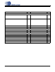
1. PIN DESCRIPTION
Pin Name # Pin Description
VD 4
Digital Power (Input) - Positive power supply for the digital section. Refer to the Recom-
mended Operating Conditions for appropriate voltages.
GND 5,31 Ground (Input) - Ground reference. Should be connected to analog ground.
MCLK 6
Master Clock (Input) - Clock source for the delta-sigma modulator and digital filters. Table 1
illustrates several standard audio sample rates and the required master clock frequencies.
LRCK 7
Left Right Clock (Input) - Determines which channel, Left or Right, is currently active on the
serial audio data line. The frequency of the left/right clock must be at the audio sample rate, Fs.
SDIN1
SDIN2
SDIN3
8
11
13
Serial Data Input (Input) - Input for two’s complement serial audio data.
SCLK 9 Serial Clock (Input) - Serial clocks for the serial audio interface.
TST
10,12
14,44
45
Test - These pin s ne ed to be tied to analog ground.
RST
19
Reset (Input) - The device enters a low power mode and all internal registers are reset to their
default settings when low.
VA 32
Analog Power (Input) - Positive power supply for the analog section. Refer to the Recom-
mended Operating Conditions for appropriate voltages.
VLS 43
Serial Audio Interface Power (Input) - Determines the required signal level for the serial audio
interface. Refer to the Recommended Operating Conditions for appropriate voltages.
VLC 18
Control Port Power (Input) - Determines the required signal level for the control port and hard-
ware mode configuration pins. Refer to the Recommended Operating C onditions for appropri-
ate voltages.
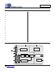
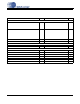
SDIN3
GND
AOUTB2-
AOUTA3+
AOUTB3-
AOUTB2+
VA
AOUTA3-
AOUTB3+
MUTEC2
MUTEC3
6
2
4
8
10
1
3
5
7
9
11
1
2
13 14 15 16 17 18 19 20 21 22 23 24
31
35
33
29
27
36
34
32
30
28
26
25
48 47 46 45 44 43 42 41 40 39 38 37
MCLK
DSDB1
VD
SDIN1
TST
DSDA2
DSDA1
GND
SCLK
SDIN2
TST
LRCK(DSD_EN)
M3(DSD_SCLK)
DSDB3
DSDA3
TST
CS4362A
TST
VLS
TST
M2(SCL/CCLK)
M1(SDA/CDIN)
VLC
RST
FILT+
VQ
MUTEC6
MUTEC5
MUTEC4
M0(AD0/CS)
AOUTA2+
AOUTA2-
AOUTB1+
AOUTB1-
AOUTA1-
AOUTA1+
DSDB2
MUTEC1