
Manual


DS257F2 31
CS4362
7.4 SPI Format
In SPI format, CS is the CS4362 chip select signal, CCLK is the control port bit clock, CDIN is the input data
line from the microcontroller and the chip address is 0011000. CS
, CCLK and CDIN are all inputs and data
is clocked in on the rising edge of CCLK.
Note: The CS4362 is write-only when in SPI format.
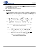
7.4.1 Writing in SPI
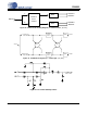
Figure 8 shows the operation of the control port in SPI format. To write to a register, bring CS low. The
first 7 bits on CDIN form the chip address and must be 0011000. The eighth bit is a read/write indicator
(R/W
), which must be low to write. The next 8 bits form the Memory Address Pointer (MAP), which is set
to the address of the register that is to be updated. The next 8 bits are the data which will be placed into
register designated by the MAP. To write multiple registers, keep CS
low and continue providing clocks
on CCLK. End the read transaction by setting CS
high.
SDA
SCL
001100
ADDR
AD0
R/W
Start
ACK
DATA
1-8
ACK
DATA
1-8
ACK
Stop
Note: If operation is a write, this byte contains the Memory Address Pointer, MAP.
Note 1
Figure 7. Control Port Timing, I²C Format
MAP
MSB
LSB
DATA
byte 1
byte n
R/W
M AP = M em ory Address Pointer
ADDRESS
CHIP
CDIN
CCLK
CS
0011000
Figure 8. Control Port Timing, SPI Format