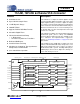
CS4362 114 dB, 192 kHz 6-Channel D/A Converter Features Description 24-bit Conversion The CS4362 is a complete 6-channel digital-to-analog system including digital interpolation, fifth-order deltasigma digital-to-analog conversion, digital de-emphasis, volume control and analog filtering. The advantages of this architecture include: ideal differential linearity, no distortion mechanisms due to resistor matching errors, no linearity drift over time and temperature and a high tolerance to clock jitter.
CS4362 TABLE OF CONTENTS 1. CHARACTERISTICS AND SPECIFICATIONS ..................................................................................... 5 ANALOG CHARACTERISTICS............................................................................................................. 5 ANALOG CHARACTERISTICS............................................................................................................. 6 POWER AND THERMAL CHARACTERISTICS ...........................................................
CS4362 6.2 PCM Mode Select ......................................................................................................................... 28 6.3 Recommended Power-Up Sequence ........................................................................................... 28 6.4 Analog Output and Filtering .......................................................................................................... 28 6.5 Interpolation Filter ................................................................
CS4362 Figure 27. Quad-Speed (fast) Transition Band .......................................................................................... 36 Figure 28. Quad-Speed (fast) Passband Ripple ........................................................................................ 36 Figure 29. Quad-Speed (slow) Stopband Rejection................................................................................... 36 Figure 30. Quad-Speed (slow) Transition Band...................................................
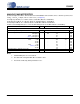
CS4362 1. CHARACTERISTICS AND SPECIFICATIONS ANALOG CHARACTERISTICS (Full-Scale Output Sine Wave, 997 Hz; Measurement Bandwidth 10 Hz to 20 kHz, unless otherwise specified; Test load RL = 3 kΩ, CL = 100 pF, VA = 5 V, VD = 3.3 V (see Figure 5) For Single-Speed Mode, Fs = 48 kHz, SCLK = 3.072 MHz, MCLK = 12.288 MHz; For Double-Speed Mode, Fs = 96 kHz, SCLK = 6.144 MHz, MCLK = 12.288 MHz; For Quad-Speed Mode, Fs = 192 kHz, SCLK = 12.288 MHz, MCLK = 24.
CS4362 ANALOG CHARACTERISTICS (Continued) Parameters Analog Output - All PCM modes and DSD Full Scale Differential Output Voltage Quiescent Voltage Max Current from VQ Interchannel Gain Mismatch Gain Drift Output Impedance AC-Load Resistance Load Capacitance (Note 4) (Note 4) Symbol Min Typ Max Units VFS VQ IQMAX 86% VA - 91% VA 50% VA 1 96% VA - Vpp VDC μA ZOUT RL CL 3 - 0.
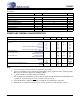
CS4362 ANALOG FILTER RESPONSE Fast Roll-Off Slow Roll-Off (Note 10) Parameter Min Typ Max Min Typ Max Combined Digital and On-chip Analog Filter Response - Single-Speed Mode (Note 11) Passband (Note 12) to -0.01 dB corner to -3 dB corner Frequency Response 10 Hz to 20 kHz StopBand StopBand Attenuation (Note 13) Group Delay Passband Group Delay Deviation 0 - 20 kHz De-emphasis Error (Note 14) Fs = 32 kHz (Relative to 1 kHz) Fs = 44.
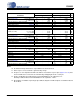
CS4362 DIGITAL CHARACTERISTICS (For KQZ TA = -10°C to +70°C; VLC = VLS = 1.8 V to 5.
CS4362 SWITCHING CHARACTERISTICS (For KQZ TA = -10°C to +70°C; VLS = 1.8 V to 5.5 V; Inputs: Logic 0 = GND, Logic 1 = VLS, CL = 30 pF) Parameters Symbol Min Typ Max Units 1.024 - 51.2 MHz Double-Speed Mode 6.400 - 51.2 MHz Quad-Speed Mode 6.400 - 51.
CS4362 DSD - SWITCHING CHARACTERISTICS (TA= -10°C to 70°C; Logic 0 = GND; VLS = 1.8 V to 5.5 V; Logic 1 = VLS Volts; CL = 30 pF) Parameter Master Clock Frequency MCLK Duty Cycle modes) DSD_SCLK Pulse Width Low DSD_SCLK Pulse Width High DSD_SCLK Frequency pled) Symbol Min Typ Max Unit 4.096 40 50 38.4 60 MHz % tsclkl tsclkh 20 20 1.024 2.048 - 3.2 6.
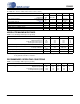
CS4362 SWITCHING CHARACTERISTICS - CONTROL PORT - I²C® FORMAT (For KQZ TA = -10°C to +70°C; VLC = 1.8 V to 5.5 V; Inputs: Logic 0 = GND, Logic 1 = VLC, CL = 30 pF) Symbol Min Max Unit SCL Clock Frequency Parameter fscl - 100 kHz RST Rising Edge to Start tirs 500 - ns Bus Free Time Between Transmissions tbuf 4.7 - µs Start Condition Hold Time (prior to first clock pulse) thdst 4.0 - µs Clock Low time tlow 4.7 - µs Clock High Time thigh 4.
CS4362 SWITCHING CHARACTERISTICS - CONTROL PORT - SPI™ FORMAT (For KQZ TA = -10°C to +70°C; VLC = 1.8 V to 5.5 V; Inputs: Logic 0 = GND, Logic 1 = VLC, CL = 30 pF) Parameter Symbol Min Max Unit - MCLK ----------------2 MHz CCLK Clock Frequency fsclk RST Rising Edge to CS Falling tsrs 500 - ns tspi 500 - ns CS High Time Between Transmissions tcsh 1.
CS4362 2. TYPICAL CONNECTION DIAGRAM +5 V +3.3 V to +5 V 1 µF + 0.1 µF 0.1 µF 4 VD 6 7 9 PCM D igital A udio S ource 10 12 8 11 13 +1.
CS4362 +3.3 V to +5 V +5 V + 1 µF 4 VD VLS Note DSD + 0.1 µF 0.
CS4362 3. REGISTER QUICK REFERENCE Addr Function 01h Mode Control 1 02h Mode Control 2 03h Mode Control 3 04h Filter Control 05h Invert Control 06h Mixing Control Pair 1 (AOUTx1) 07h Vol. Control A1 08h Vol. Control B1 default default default default default default default default 09h Mixing Control Pair 2 (AOUTx2) default 0Ah Vol. Control A2 default 0Bh Vol. Control B2 default 0Ch Mixing Control Pair 3 (AOUTx3) default 0Dh Vol. Control A3 default 0Eh Vol.
CS4362 4. REGISTER DESCRIPTION Note: All registers are read/write in I²C Mode and write-only in SPI, unless otherwise noted. 4.1 Mode Control 1 (address 01h) 7 CPEN 0 4.1.1 6 FREEZE 0 5 MCLKDIV 0 4 Reserved 0 3 DAC3_DIS 0 2 DAC2_DIS 0 1 DAC1_DIS 0 0 PDN 1 Control Port Enable (CPEN) Default = 0 0 - Disabled 1 - Enabled Function: This bit defaults to 0, allowing the device to power-up in Stand-Alone Mode. The Control Port Mode can be accessed by setting this bit to 1.
CS4362 4.1.5 Power Down (PDN) Default = 1 0 - Disabled 1 - Enabled Function: The entire device will enter a low-power state when this function is enabled, and the contents of the control registers are retained in this mode. The power-down bit defaults to ‘enabled’ on power-up and must be disabled before normal operation in Control Port Mode can occur. 4.2 Mode Control 2 (address 02h) 7 Reserved 0 4.2.
CS4362 DSD Mode: The relationship between the oversampling ratio of the DSD audio data and the required Master clock to DSD data rate is defined by the Digital Interface Format pins. An additional write of 99h to register 00h and 80h to register 1Ah is required to access the modes denoted with *.
CS4362 Soft Ramp Soft Ramp allows level changes, both muting and attenuation, to be implemented by incrementally ramping, in 1/8 dB steps, from the current level to the new level at a rate of 1 dB per 8 left/right clock periods. Soft Ramp on Zero Crossing Soft Ramp and Zero Cross Enable dictates that signal level changes, either by attenuation changes or muting, will occur in 1/8 dB steps and be implemented on a signal zero crossing.
CS4362 4.3.5 Auto-Mute (AMUTE) Default = 1 0 - Disabled 1 - Enabled Function: The Digital-to-Analog converter output will mute following the reception of 8192 consecutive audio samples of static 0 or -1. A single sample of non-static data will release the mute. Detection and muting is done independently for each channel. The quiescent voltage on the output will be retained and the Mute Control pin will go active during the mute period.
CS4362 Selects the appropriate digital filter to maintain the standard 15 μs/50 μs digital de-emphasis filter response at 32, 44.1 or 48 kHz sample rates. (see Figure 39) De-emphasis is only available in Single-Speed Mode. 4.4.3 Soft Ramp-Down Before Filter Mode Change (RMP_DN) Default = 0 0 - Disabled 1 - Enabled Function: A mute will be performed prior to executing a filter mode change.
CS4362 4.6.2 ATAPI Channel Mixing and Muting (ATAPI) Default = 01001 - AOUTAx=aL, AOUTBx=bR (Stereo) Function: The CS4362 implements the channel mixing functions of the ATAPI CD-ROM specification. The ATAPI functions are applied per A-B pair. Refer to Table 3 and Figure 41 for additional information.
CS4362 4.6.3 Functional Mode (FM) Default = 00 00 - Single-Speed Mode (4 to 50 kHz sample rates) 01 - Double-Speed Mode (50 to 100 kHz sample rates) 10 - Quad-Speed Mode (100 to 200 kHz sample rates) 11 - Direct Stream Digital Mode Function: Selects the required range of input sample rates or DSD Mode. All DAC pairs set to the same SCLK/LRCK pair (Section 4.2.2) are required to be set to the same functional mode setting before a speed mode change is accepted.
CS4362 4.8 Chip Revision (address 12h) 7 PART3 1 4.8.1 6 PART2 1 5 PART1 1 4 PART0 0 3 Reserved - 2 Reserved - 1 Reserved - 0 Reserved - Part Number ID (PART) [Read Only] 1110 - CS4362 Function: This read-only register can be used to identify the model number of the device.
CS4362 AOUTB1- AOUTB1+ AOUTA1+ AOUTA1- M UTEC1 VLS M 3(DSD_SCLK) TST TST DSDB3 DSDA3 DSDB2 5.
CS4362 Pin Name # Pin Description VQ 21 Quiescent Voltage (Output) - Filter connection for internal quiescent voltage. VQ must be capacitively coupled to analog ground, as shown in the Typical Connection Diagram. The nominal voltage level is specified in the Analog Characteristics and Specifications section. VQ presents an appreciable source impedance and any current drawn from this pin will alter device performance.
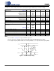
CS4362 Sample Rate (kHz) Mode (sample-rate range) MCLK Ratio Single-Speed (4 to 50 kHz) 256x 8.1920 11.2896 12.2880 128x 8.1920 11.2896 12.2880 64x 11.2896 12.2880 32 44.1 48 MCLK Ratio Double-Speed (50 to 100 kHz) Control Port Only Modes MCLK (MHz) 64 88.2 96 MCLK Ratio 176.4 Quad-Speed (100 to 200 kHz) 192 384x 12.2880 16.9344 18.4320 192x 12.2880 16.9344 18.4320 96x 16.9344 18.4320 512x 16.3840 22.5792 24.5760 256x 16.3840 22.5792 24.5760 128x 22.5792 24.5760 768x 24.5760 33.8688 36.
CS4362 6. APPLICATIONS 6.1 Grounding and Power Supply Decoupling As with any high resolution converter, the CS4362 requires careful attention to power supply and grounding arrangements to optimize performance. Figures 5 and 6 show the recommended power arrangement with VA, VD, VLS and VLC connected to clean supplies. Decoupling capacitors should be located as close to the device package as possible.
CS4362 variety of musical tastes and styles. The FILT_SEL bit is used to select which filter is used (see the control port section for more details). When in Stand-Alone Mode, only the “fast” roll-off filter is available. Filter specifications can be found in Section 1, and filter response plots can be found in Figures 9 to 32. 6.6 Clock Source Selection The CS4362 has two serial clock and two left/right clock inputs.
CS4362 7. CONTROL PORT INTERFACE The control port is used to load all the internal settings. The operation of the control port may be completely asynchronous with the audio sample rate. However, to avoid potential interference problems, the control port pins should remain static if no operation is required. The CS4362 has MAP auto increment capability, enabled by the INCR bit in the MAP register, which is the MSB. If INCR is 0, then the MAP will stay constant for successive writes.
CS4362 7.4 SPI Format In SPI format, CS is the CS4362 chip select signal, CCLK is the control port bit clock, CDIN is the input data line from the microcontroller and the chip address is 0011000. CS, CCLK and CDIN are all inputs and data is clocked in on the rising edge of CCLK. Note: 7.4.1 The CS4362 is write-only when in SPI format. Writing in SPI Figure 8 shows the operation of the control port in SPI format. To write to a register, bring CS low.
CS4362 7.5 Memory Address Pointer (MAP) 7 INCR 0 7.5.1 6 Reserved 0 5 Reserved 0 4 MAP4 0 3 MAP3 0 2 MAP2 0 1 MAP1 0 0 MAP0 0 INCR (Auto Map Increment Enable) Default = ‘0’ 0 - Disabled 1 - Enabled Note: When Auto Map Increment is enabled, the register must be written it two separate blocks: from register 01h to 08h and then from 09h and 11h. The counter will not auto-increment to register 09h from register 08h 7.5.
CS4362 8. FILTER PLOTS 0 20 20 40 40 Amplitude (dB) Amplitude (dB) 0 60 60 80 80 100 100 120 120 0.4 0.5 0.6 0.7 0.8 Frequency(normalized to Fs) 0.9 1 Figure 9. Single-Speed (fast) Stopband Rejection 0.4 0.42 0.44 0.46 0.48 0.5 0.52 Frequency(normalized to Fs) 0.54 0.56 0.58 0.6 Figure 10. Single-Speed (fast) Transition Band 0.02 0 1 0.015 2 0.01 0.005 4 Amplitude (dB) Amplitude (dB) 3 5 6 0 0.005 7 0.01 8 0.015 9 10 0.45 0.46 0.47 0.48 0.49 0.5 0.
CS4362 0.02 0 1 0.015 2 0.01 3 Amplitude (dB) Amplitude (dB) 0.005 4 5 6 0 0.005 7 0.01 8 0.015 9 10 0.45 0.02 0.46 0.47 0.48 0.49 0.5 0.51 Frequency(normalized to Fs) 0.52 0.53 0.54 0.55 Figure 15. Single-Speed (slow) Transition Band (detail) 0.1 0.15 0.2 0.25 0.3 Frequency(normalized to Fs) 0.35 0.4 0.45 0.5 0 20 20 40 40 Amplitude (dB) Amplitude (dB) 0.05 Figure 16. Single-Speed (slow) Passband Ripple 0 60 60 80 80 100 100 120 0 120 0.4 0.5 0.6 0.7 0.
CS4362 0 20 20 40 40 Amplitude (dB) Amplitude (dB) 0 60 60 80 80 100 100 120 120 0.2 0.3 0.4 0.5 0.6 0.7 Frequency(normalized to Fs) 0.8 0.9 1 Figure 21. Double-Speed (slow) Stopband Rejection 0.2 0.3 0.4 0.5 0.6 Frequency(normalized to Fs) 0.7 0.8 Figure 22. Double-Speed (slow) Transition Band 0.02 0 1 0.015 2 0.01 3 Amplitude (dB) Amplitude (dB) 0.005 4 5 6 0 0.005 7 0.01 8 0.015 9 10 0.45 0.02 0.46 0.47 0.48 0.49 0.5 0.51 Frequency(normalized to Fs) 0.
CS4362 0.2 0 1 0.15 2 0.1 3 Amplitude (dB) Amplitude (dB) 0.05 4 5 6 0 0.05 7 0.1 8 0.15 9 10 0.45 0.2 0.46 0.47 0.48 0.49 0.5 0.51 Frequency(normalized to Fs) 0.52 0.53 0.54 0.55 Figure 27. Quad-Speed (fast) Transition Band 0 0.05 0.1 0.15 Frequency(normalized to Fs) 0.2 0.25 Figure 28. Quad-Speed (fast) Passband Ripple 0 0 20 40 40 Amplitude (dB) Amplitude (dB) 20 60 60 80 80 100 100 120 120 0.1 0.2 0.3 0.4 0.5 0.6 0.7 Frequency(normalized to Fs) 0.
CS4362 9. DIAGRAMS Left Channel LRCK Right Channel SCLK SDINx MSB -1 -2 -3 -4 -5 +5 +4 +3 +2 +1 LSB MSB -1 -2 -3 -4 +5 +4 +3 +2 +1 LSB Figure 33. Format 0 - Left Justified up to 24-bit Data Left Channel LRCK Right Channel SCLK SDINx MSB -1 -2 -3 -4 -5 +5 +4 +3 +2 +1 LSB MSB -1 -2 -3 -4 +5 +4 +3 +2 +1 LSB Figure 34.
CS4362 LRCK Right Channel Left Channel SCLK SDINx 1 0 19 18 17 16 15 14 13 12 11 10 9 8 7 6 5 4 3 2 1 0 19 18 17 16 15 14 13 12 11 10 9 8 7 6 5 4 3 2 1 0 32 clocks Figure 37. Format 4 - Right Justified 20-bit Data LRCK Right Channel Left Channel SCLK SDINx 1 0 17 16 15 14 13 12 11 10 9 8 7 6 5 4 3 2 1 0 17 16 15 14 13 12 11 10 9 8 7 6 5 4 3 2 1 0 32 clocks Figure 38. Format 5 - Right Justified 18-bit Data Gain dB T1=50 µs 0dB T2 = 15 µs -10dB F1 3.183 kHz F2 Frequency 10.
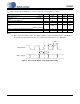
CS4362 L AOUTAx+ AOUTAx- DAC Channel Pair x Control SDINx R AOUTBx+ DAC AOUTBx- Figure 40. Channel Pair Routing Diagram (x = Channel Pair 1, 2, or 3) A Channel Volume Control Left Channel Audio Data Σ SDINx Right Channel Audio Data MUTE Aout Ax MUTE AoutBx Σ B Channel Volume Control Figure 41. ATAPI Block Diagram (x = channel pair 1, 2, or 3) Figure 42.
CS4362 10.PARAMETER DEFINITIONS Total Harmonic Distortion + Noise (THD+N) The ratio of the rms value of the signal to the rms sum of all other spectral components over the specified bandwidth (typically 10 Hz to 20 kHz), including distortion components. Expressed in decibels. Dynamic Range The ratio of the full-scale rms value of the signal to the rms sum of all other spectral components over the specified bandwidth.
CS4362 12.PACKAGE DIMENSIONS 48L LQFP PACKAGE DRAWING E E1 D D1 1 e B ∝ A A1 L DIM A A1 B D D1 E E1 e* L ∝ MIN --0.002 0.007 0.343 0.272 0.343 0.272 0.016 0.018 0.000° INCHES NOM 0.055 0.004 0.009 0.354 0.28 0.354 0.28 0.020 0.24 4° MAX 0.063 0.006 0.011 0.366 0.280 0.366 0.280 0.024 0.030 7.000° MIN --0.05 0.17 8.70 6.90 8.70 6.90 0.40 0.45 0.00° MILLIMETERS NOM 1.40 0.10 0.22 9.0 BSC 7.0 BSC 9.0 BSC 7.0 BSC 0.50 BSC 0.60 4° MAX 1.60 0.15 0.27 9.30 7.10 9.30 7.10 0.60 0.75 7.
CS4362 13. ORDERING INFORMATION Product Description Package Pb-Free 114 dB, 192 kHz 648-pin CS4362 channel D/A Converter LQFP CDB4362 CS4362 Evaluation Board YES - Grade Temp Range Commercial -10°C to +70°C - - Container Order # Tray Tape and Reel - CS4362-KQZ CS4362-KQZR CDB4362 14.