
Instruction Manual


11
CS4361
Confidential Draft
9/30/11
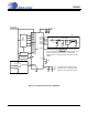
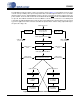
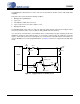
3. TYPICAL CONNECTION DIAGRAM
DEM/SCLK
14
Audio
Data
Processor
External Clock
MCLK
GND
CS4361
SDIN1
LRCK
VL
AOUT1
6
2
5
7
1
0.1 µF
+
1µF
19
Audio Output
+5 V
3.3 µF
10 k
C
470
+
R + 470
C=
4
Fs(R 470)
R
ext
ext
ext
+
0.1 µF
33
+
µF
10
VQ
FILT+
11
Note*
Note* = This circuitry is intended for applications where the CS4361 connects
directly to an unbalanced output of the design. For internal routing
applications please see the DAC analog output characteristics for loading
limitations.
For best 20 kHz response
SDIN2
3
SDIN3
4
20
MUTEC
AOUT2
18
AOUT3
17
AOUT4
16
AOUT5
13
AOUT6
12
Optional
Muting
Circuit
RST
8
Controler
MODE
9
+1.8 V to +5 V
VA
15
VL
GND
LRCK
LJ
RJ16
RJ24
I
2
S
MCLK
µF*3.3
µF*10
*Popguard ramp can be adjusted by selecting
this capacitor value to be 3.3 µF to give 250 ms
ramp time or 10 µF to give a 420 ms ramp time.
or
Figure 6. Recommended Connection Diagram