
Manual

DS566F1 5
CS4351
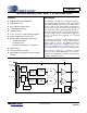
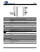
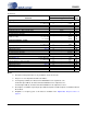
1. PIN DESCRIPTION
Pin Name # Pin Description
SDIN 1 Serial Audio Data Input (Input) - Input for two’s complement serial audio data.
SCLK 2 Serial Clock (Input) - Serial clock for the serial audio interface.
LRCK 3
Left / Right Clock (Input) - Determines which channel, Left or Right, is currently active on the serial
audio data line.
MCLK 4 Master Clock (Input) - Clock source for the delta-sigma modulator and digital filters.
VD 5 Digital Power (Input) - Positive power supply for the digital section.
GND
6
16
Ground (Input) - Ground reference.
RST
10
Reset (Input) - Powers down device and resets all internal resisters to their default settings when
enabled.
VA 11 Low Voltage Analog Power (Input) - Positive power supply for the analog section.
VBIAS 12 Positive Voltage Reference (Output) - Positive reference voltage for the internal DAC.
VQ 13 Quiescent Voltage (Output) - Filter connection for internal quiescent voltage.
VA_H 17 High Voltage Analog Power (Input) - Positive power supply for the analog section.
VL 20 Serial Audio Interface Power (Input) - Positive power for the serial audio interface
BMUTEC
AMUTEC
14
19
Mute Control (Output) - Control signal for optional mute circuit.
AOUTB
AOUTA
15
18
Analog Outputs (Output) - The full scale analog line output level is specified in the Analog Character-
istics table.
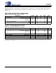
Control Port Definitions
SCL/CCLK 7 Serial Control Port Clock (Input) - Serial clock for the control port interface.
SDA/CDIN 8 Serial Control Data (Input/Output) - Input/Output for I²C data. Input for SPI data.
AD0/CS
9 Address Bit 0 / Chip Select (Input) - Chip address bit in I²C Mode. Control Port enable in SPI Mode.
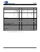
Stand-Alone Definitions
DIF0
DIF1
8
7
Digital Interface Format (Input) - Defines the required relationship between the Left Right Clock,
Serial Clock, and Serial Audio Data.
DEM 9
De-emphasis (Input) - Selects the standard 15 µs/50 µs digital de-emphasis filter response for 44.1
kHz sample rates
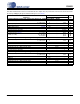
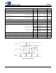
SDIN VL
SCLK AMUTEC
LRCK AOUTA
MCLK VA_H
VD GND
GND AOUTB
DIF1(SCL/CCLK) BMUTEC
DIF0(SDA/CDIN) VQ
DEM(AD0/CS
) VBIAS
RST
VA
1
2
3
4
5
6
7
8
9
10
11
12
17
18
19
20
13
14
15
16