
Manual

DS566F1 13
CS4351
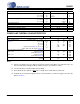
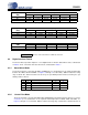
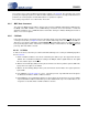
DIGITAL CHARACTERISTICS
POWER AND THERMAL CHARACTERISTICS
Notes:
11. Current consumption increases with increasing FS and increasing MCLK. Typ and Max values are
based on highest FS and highest MCLK. Variance between speed modes is small.
12. I
L
measured with no external loading on pin 8 (SDA).
13. Power-Down Mode is defined as RES
pin = Low with all clock and data lines held static.
14. Valid with the recommended capacitor values on VQ and V
BIAS
as shown in the typical connection dia-
gram in Section 3.
Parameters Symbol Min Typ Max Units
High-Level Input Voltage VL = 3.3 V
VL = 2.5 V
VL = 1.8 V
V
IH
V
IH
V
IH
2.0
1.7
0.65•V
L
-
-
-
-
-
-
V
V
V
Low-Level Input Voltage VL = 3.3 V
VL = 2.5 V
VL = 1.8 V
V
IL
V
IL
V
IL
-
-
-
-
-
-
0.8
0.7
0.33•V
L
V
V
V
Input Leakage Current I
in
--±10µA
Input Capacitance - 8 - pF
Maximum MUTEC Drive Current - 2 - mA
MUTEC High-Level Output Voltage V
OH
-VA_H- V
MUTEC Low-Level Output Voltage V
OL
-0- V
Parameters Symbol Min Typ Max Units
Power Supplies
Power Supply Current normal operation, V
A_H
= 12 V
(Note 11) V
A_H
= 9 V
V
A
= 3.3 V
V
D
= 3.3 V
Interface current (Note 12) V
L
= 3.3 V
power-down state, all supplies (Note 13)
I
A_H
I
A_H
I
A
I
D
I
L
I
pd
-
-
-
-
-
-
15
14
6
21
100
200
20
19
8
26
400
-
mA
mA
mA
mA
µA
µA
Power Dissipation (all supplies) (Note 11)
VA_H = 12 V normal operation
power-down (Note 13)
VA_H = 9 V normal operation
power-down (Note 13)
-
-
-
-
270
1
216
1
354
-
285
-
mW
mW
mW
mW
Power Supply Rejection Ratio (Note 14) (1 kHz)
(60 Hz)
PSRR -
-
60
60
-
-
dB
dB