CS4351 192 kHz Stereo DAC with 2 Vrms Line Out Features Description ! Multi-Bit Delta-Sigma Modulator The CS4351 is a complete stereo digital-to-analog system including digital interpolation, fifth-order multi-bit delta-sigma digital-to-analog conversion, digital de-emphasis, volume control, channel mixing, analog filtering, and on-chip 2 Vrms line-level driver.
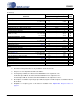
CS4351 TABLE OF CONTENTS 1. PIN DESCRIPTION ............................................................................................................................... 5 2. CHARACTERISTICS AND SPECIFICATIONS ..................................................................................... 6 SPECIFIED OPERATING CONDITIONS .............................................................................................. 6 ABSOLUTE MAXIMUM RATINGS ...........................................................
CS4351 6.3.4 ATAPI Channel Mixing and Muting (ATAPI3:0) Bits 3-0 .................................................. 26 6.4 Mute Control - Register 04h ........................................................................................................ 27 6.4.1 Auto-Mute (AMUTE) Bit 7 ................................................................................................ 27 6.4.2 AMUTEC = BMUTEC (MUTEC A=B) Bit 5 ...................................................................... 27 6.4.
CS4351 Figure 29.Quad-Speed (fast) Stopband Rejection ..................................................................................... 33 Figure 30.Quad-Speed (fast) Transition Band ........................................................................................... 33 Figure 31.Quad-Speed (fast) Transition Band (detail) ............................................................................... 34 Figure 32.Quad-Speed (fast) Passband Ripple ..................................................
CS4351 1. PIN DESCRIPTION SDIN SCLK LRCK MCLK VD GND DIF1(SCL/CCLK) DIF0(SDA/CDIN) DEM(AD0/CS) RST Pin Name 1 20 2 19 3 18 4 17 5 16 6 15 7 14 8 13 9 12 10 11 # VL AMUTEC AOUTA VA_H GND AOUTB BMUTEC VQ VBIAS VA Pin Description SDIN 1 Serial Audio Data Input (Input) - Input for two’s complement serial audio data. SCLK 2 Serial Clock (Input) - Serial clock for the serial audio interface.
CS4351 2. CHARACTERISTICS AND SPECIFICATIONS (Min/Max performance characteristics and specifications are guaranteed over the Specified Operating Conditions. Typical specifications are derived from performance measurements at TA = 25 °C, VA_H = 12 V, VA = 3.3 V, VD = 3.3 V.) SPECIFIED OPERATING CONDITIONS (GND = 0 V; all voltages with respect to ground.
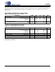
CS4351 DAC ANALOG CHARACTERISTICS (Test conditions (unless otherwise specified): input test signal is a 997 Hz sine wave at 0 dBFS; measurement bandwidth 10 Hz to 20 kHz) Parameter All Speed Modes Dynamic Range (Note 1) Symbol Min Typ Max Unit 99 102 - 109 112 95 98 - dB dB dB dB - -100 -89 -49 -92 -75 -35 -90 -79 -39 - dB dB dB dB dB dB - 109 - dB - 100 - dB 1.85 2.00 2.
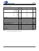
CS4351 COMBINED INTERPOLATION & ON-CHIP ANALOG FILTER RESPONSE (The filter characteristics have been normalized to the sample rate (Fs) and can be referenced to the desired sample rate by multiplying the given characteristic by Fs.
CS4351 COMBINED INTERPOLATION & ON-CHIP ANALOG FILTER RESPONSE (Continued) Slow Roll-Off (Note 2) Min Typ Max Parameter Single-Speed Mode - 48 kHz Passband (Note 3) Frequency Response 10 Hz to 20 kHz StopBand StopBand Attenuation Total Group Delay (Fs = Output Sample Rate) Intra-channel Phase Deviation Inter-channel Phase Deviation De-emphasis Error (Note 5) (Relative to 1 kHz) to -0.01 dB corner to -3 dB corner (Note 4) Fs = 32 kHz Fs = 44.1 kHz Fs = 48 kHz Unit 0 0 -0.01 .583 64 - 6.5/Fs - 0.
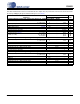
CS4351 SWITCHING SPECIFICATIONS - SERIAL AUDIO INTERFACE Parameters Min Max Units MCLK Frequency 1.024 51.
CS4351 Switching Characteristics - Control Port - I²C® Format (Inputs: Logic 0 = GND, Logic 1 = VL, CL = 20 pF) Symbol Min Max Unit SCL Clock Frequency Parameter fscl - 100 kHz RST Rising Edge to Start tirs 500 - ns Bus Free Time Between Transmissions tbuf 4.7 - µs Start Condition Hold Time (prior to first clock pulse) thdst 4.0 - µs Clock Low time tlow 4.7 - µs Clock High Time thigh 4.0 - µs tsust 4.
CS4351 SWITCHING CHARACTERISTICS - CONTROL PORT - SPI™ FORMAT (Inputs: Logic 0 = GND, Logic 1 = VL, CL = 20 pF) Parameter Symbol Min Max Unit CCLK Clock Frequency fsclk - 6 MHz RST Rising Edge to CS Falling tsrs 500 - ns tspi 500 - ns CS High Time Between Transmissions tcsh 1.
CS4351 DIGITAL CHARACTERISTICS Parameters High-Level Input Voltage Symbol Min Typ Max Units VIH VIH VIH VIL VIL VIL Iin 2.0 1.7 0.65•VL - 8 2 VA_H 0 0.8 0.7 0.33•VL ±10 - V V V V V V µA pF mA V V VL = 3.3 V VL = 2.5 V VL = 1.8 V VL = 3.3 V VL = 2.5 V VL = 1.
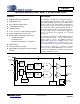
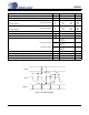
CS4351 3. TYPICAL CONNECTION DIAGRAM 5.1Ω∗ +3.3 V +3.3 V * *Remove this supply if optional resistor is present. The decoupling caps should remain. 10 µF + *Optional + 0.1 µF 0.1 µF 10 µF 11 VA 5 VD + 3.3 µF VBIAS+ 12 4 Digital Audio Source 3 2 1 MCLK LRCK VA_H 17 +9 V to +12 V 0.1 µF SCLK + 10 µF SDIN Optional Mute Circuit +1.8 V to VD 20 AMUTEC 19 VL 0.1 µF AOUTA + 3.3 µF CS4351 576 k Ω 560 Ω 18 412 k Ω AOUTA 10 k Ω 2.
CS4351 4. APPLICATIONS 4.1 Sample Rate Range/Operational Mode Detect The device operates in one of three operational modes. The allowed sample rate range in each mode will depend on whether the Auto-Detect Defeat bit is enabled/disabled. 4.1.1 Auto-Detect Enabled The Auto-Detect feature is enabled by default. In this state, the CS4351 will auto-detect the correct mode when the input sample rate (Fs), defined by the LRCK frequency, falls within one of the ranges illustrated in Table 1.
CS4351 Sample Rate (kHz) MCLK (MHz) 512x 768x 256x 384x 32 44.1 48 8.1920 11.2896 12.2880 12.2880 16.9344 18.4320 16.3840 22.5792 24.5760 24.5760 33.8688 36.8640 1024x 1152x 32.7680 45.1584 49.1520 36.8640 Table 3. Single-Speed Mode Standard Frequencies Sample Rate (kHz) 128x 192x 64 88.2 96 8.1920 11.2896 12.2880 12.2880 16.9344 18.4320 MCLK (MHz) 256x 16.3840 22.5792 24.5760 384x 512x 24.5760 33.8688 36.8640 32.7680 45.1584 49.1520 Table 4.
CS4351 least 32 cycles per LRCK period in format 2, 48 cycles in format 3, 40 cycles in format 4, and 36 cycles in format 5. Left C ha nnel LR C K R ig ht C ha nnel S C LK SDIN MSB -1 -2 -3 -4 -5 +5 +4 +3 +2 +1 MSB LSB -1 -2 -3 -4 +5 +4 +3 +2 +1 LSB Figure 5. Left-Justified up to 24-Bit Data Left Channel LR C K R ight C ha nnel S C LK SDIN M SB -1 -2 -3 -4 -5 +5 +4 +3 +2 +1 LSB M SB -1 -2 -3 -4 +5 +4 +3 +2 +1 LSB Figure 6.
CS4351 4.4.1 Stand-Alone Mode When pulled to VL the DEM pin activates the 44.1 kHz de-emphasis filter. When pulled to GND the DEM pin turns off the de-emphasis filter. 4.4.2 Control Port Mode The Mode Control bits selects either the 32, 44.1, or 48 kHz de-emphasis filter. Please see Section 6.2.2 for the desired de-emphasis control. 4.5 4.5.1 Recommended Power-Up Sequence Stand-Alone Mode 1.
CS4351 4.6.2 Power-Down To prevent audible transients at power-down, the device must first enter its power-down state. When this occurs, audio output ceases and the internal output buffers are disconnected from AOUTA and AOUTB. In their place, a soft-start current sink is substituted which allows the DC-blocking capacitors to slowly discharge. Once this charge is dissipated, the power to the device may be turned off and the system is ready for the next power-on. 4.6.
CS4351 4.9 Control Port Interface The control port is used to load all the internal register settings (see Section 6). The operation of the control port may be completely asynchronous with the audio sample rate. However, to avoid potential interference problems, the control port pins should remain static if no operation is required. The control port operates in one of two modes: I²C or SPI. 4.9.
CS4351 4.9.2.2 I²C Read To read from the device, follow the procedure below while adhering to the control port Switching Specifications. 1. Initiate a START condition to the I²C bus followed by the address byte. The upper 6 bits must be 100110. The seventh bit must match the setting of the AD0 pin, and the eighth must be 1. The eighth bit of the address byte is the R/W bit. 2. After transmitting an acknowledge (ACK), the device will then transmit the contents of the register pointed to by the MAP.
CS4351 4. Write the desired data to the register pointed to by the MAP. 5. If the INCR bit (see Section 4.9.1) is set to 1, repeat the previous step until all the desired registers are written, then bring CS high. 6. If the INCR bit is set to 0 and further SPI writes to other registers are desired, it is necessary to bring CS high, and follow the procedure detailed from step 1. If no further writes to other registers are desired, bring CS high.
CS4351 5. REGISTER QUICK REFERENCE Addr Function 1h Chip ID 2h Mode Control 3h Volume, Mixing, and Inversion Control default default default 4h Mute Control 5h Channel A Volume Control 6h Channel B Volume Control default default default 7h Ramp and Filter Control default 8h Misc.
CS4351 6. REGISTER DESCRIPTION ** All register access is R/W unless specified otherwise** 6.1 Chip ID - Register 01h 7 PART4 1 6 PART3 1 5 PART2 1 4 PART1 1 3 PART0 1 2 REV2 - 1 REV1 - 0 REV0 - Function: This register is Read-Only. Bits 7 through 3 are the part number ID which is 11111b and the remaining Bits (2 through 0) are for the chip revision (Rev. A = 000, Rev. B = 001, ...) 6.2 Mode Control 1 - Register 02h 7 Reserved 0 6.2.
CS4351 6.2.3 Functional Mode (FM) Bits 1-0 Default = 00 00 - Auto speed mode detect 01 - Single-Speed Mode (4 to 50 kHz sample rates) 10 - Double-Speed Mode (50 to 100 kHz sample rates) 11 - Quad-Speed Mode (100 to 200 kHz sample rates) Function: Selects the required range of input sample rates or DSD Mode. 6.3 Volume Mixing and Inversion Control - Register 03h B7 VOLB=A 0 6.3.
CS4351 6.3.4 ATAPI Channel Mixing and Muting (ATAPI3:0) Bits 3-0 Default = 1001 - AOUTA=aL, AOUTB=bR (Stereo) Function: The CS4351 implements the channel mixing functions of the ATAPI CD-ROM specification. Refer to Table 8 and Figure 12 for additional information. A Channel Volume Control Left Channel Audio Data Σ MUTE AoutA MUTE AoutB Σ B Channel Volume Control Right Channel Audio Data Figure 12.
CS4351 6.4 Mute Control - Register 04h 7 AMUTE 1 6.4.1 6 Reserved 0 5 MUTEC A=B 0 4 MUTE_A 0 3 MUTE_B 0 2 Reserved 0 1 Reserved 0 0 Reserved 0 Auto-Mute (AMUTE) Bit 7 Function: When set to 1 (default), the Digital-to-Analog converter output will mute following the reception of 8192 consecutive audio samples of static 0 or -1. A single sample of non-static data will release the mute. Detection and muting is done independently for each channel.
CS4351 6.5.1 Digital Volume Control (VOL7:0) Bits 7-0 Default = 00h (0 dB) Function: The Digital Volume Control registers allow independent control of the signal levels in 1/2 dB increments from 0 to -127.5 dB. Volume settings are decoded as shown in Table 9. The volume changes are implemented as dictated by the Soft and Zero Cross bits in the Power and Muting Control register. The actual attenuation is determined by taking the decimal value of the volume register and multiplying by 6.02/12.
CS4351 Soft Ramp and Zero Cross Soft Ramp and Zero Cross Enable dictate that signal level changes, either by attenuation changes or muting, will occur in 1/8 dB steps and be implemented on a signal zero crossing. The 1/8 dB level change will occur after a time-out period between 512 and 1024 sample periods (10.7 ms to 21.3 ms at 48 kHz sample rate) if the signal does not encounter a zero crossing. The zero cross function is independently monitored and implemented for each channel. 6.6.
CS4351 6.7.1 Power Down (PDN) Bit 7 Function: When set to 1 (default), the entire device will enter a low-power state and the contents of the control registers will be retained. The power-down bit defaults to ‘1’ on power-up and must be disabled before normal operation in Control Port mode can occur. This bit is ignored if CPEN is not set. 6.7.2 Control Port Enable (CPEN) Bit 6 Function: This bit is set to 0 by default, allowing the device to power-up in Stand-Alone Mode.
CS4351 0 0 −20 −20 −40 −40 Amplitude (dB) Amplitude (dB) 7. DIGITAL FILTER RESPONSE PLOTS −60 −60 −80 −80 −100 −100 −120 0.4 0.5 0.6 0.7 0.8 Frequency(normalized to Fs) 0.9 −120 0.4 1 Figure 13. Single-Speed (fast) Stopband Rejection 0.42 0.44 0.46 0.48 0.5 0.52 Frequency(normalized to Fs) 0.54 0.56 0.58 0.6 Figure 14. Single-Speed (fast) Transition Band 0.02 0 −1 0.015 −2 0.01 0.005 −4 Amplitude (dB) Amplitude (dB) −3 −5 −6 0 −0.005 −7 −0.01 −8 −0.
CS4351 0.02 0 −1 0.015 −2 0.01 0.005 −4 Amplitude (dB) Amplitude (dB) −3 −5 −6 0 −0.005 −7 −0.01 −8 −0.015 −9 −10 0.45 0.46 0.47 0.48 0.49 0.5 0.51 Frequency(normalized to Fs) 0.52 0.53 0.54 −0.02 0.55 Figure 19. Single-Speed (slow) Transition Band (detail) 0.1 0.15 0.2 0.25 0.3 Frequency(normalized to Fs) 0.35 0.4 0.45 0.5 0 20 20 40 40 Amplitude (dB) Amplitude (dB) 0.05 Figure 20. Single-Speed (slow) Passband Ripple 0 60 60 80 80 100 100 120 0 120 0.
CS4351 0 20 20 40 40 Amplitude (dB) Amplitude (dB) 0 60 60 80 80 100 100 120 120 0.2 0.3 0.4 0.5 0.6 0.7 Frequency(normalized to Fs) 0.8 0.9 1 Figure 25. Double-Speed (slow) Stopband Rejection 0.2 0.3 0.4 0.5 0.6 Frequency(normalized to Fs) 0.7 0.8 Figure 26. Double-Speed (slow) Transition Band 0 0.02 1 0.015 2 0.01 0.005 4 Amplitude (dB) Amplitude (dB) 3 5 6 0 0.005 7 0.01 8 0.015 9 10 0.45 0.46 0.47 0.48 0.49 0.5 0.51 Frequency(normalized to Fs) 0.52 0.
CS4351 0.2 0 1 0.15 2 0.1 3 Amplitude (dB) Amplitude (dB) 0.05 4 5 6 0 0.05 7 0.1 8 0.15 9 10 0.45 0.2 0.46 0.47 0.48 0.49 0.5 0.51 Frequency(normalized to Fs) 0.52 0.53 0.54 0.55 Figure 31. Quad-Speed (fast) Transition Band (detail) 0 0.05 0.1 0.15 Frequency(normalized to Fs) 0.2 0.25 Figure 32. Quad-Speed (fast) Passband Ripple 0 0 20 40 40 Amplitude (dB) Amplitude (dB) 20 60 60 80 80 100 100 120 120 0.1 0.2 0.3 0.4 0.5 0.6 0.
CS4351 8. PARAMETER DEFINITIONS Total Harmonic Distortion + Noise (THD+N) The ratio of the rms value of the signal to the rms sum of all other spectral components over the specified bandwidth (typically 10 Hz to 20 kHz), including distortion components. Expressed in decibels. Dynamic Range The ratio of the full scale rms value of the signal to the rms sum of all other spectral components over the specified bandwidth.
CS4351 9. PACKAGE DIMENSIONS 20L TSSOP (4.4 mm BODY) PACKAGE DRAWING N D E11 A2 E A ∝ e b2 A1 SIDE VIEW END VIEW L SEATING PLANE 1 2 3 TOP VIEW INCHES MILLIMETERS NOTE DIM MIN NOM MAX MIN NOM MAX A A1 A2 b D E E1 e L µ -0.002 0.03346 0.00748 0.252 0.248 0.169 -0.020 0° -0.004 0.0354 0.0096 0.256 0.2519 0.1732 -0.024 4° 0.043 0.006 0.037 0.012 0.259 0.256 0.177 0.026 0.028 8° -0.05 0.85 0.19 6.40 6.30 4.30 -0.50 0° --0.90 0.245 6.50 6.40 4.40 -0.60 4° 1.10 0.15 0.95 0.30 6.60 6.
CS4351 10.ORDERING INFORMATION Product CS4351 Description 192 kHz Stereo DAC with 2 Vrms Line Out CDB4351 Package Pb-Free 20-pin TSSOP CS4351 Evaluation Board Grade Temp Range Container Commercial -10° to +70° C Automotive -40° to +85° C - - YES - Rail Order # CS4351-CZZ Tape & Reel CS4351-CZZR Rail CS4351-DZZ Tape & Reel CS4351-DZZR - CDB4351 11.REVISION HISTORY Release PP3 PP4 F1 Date March 2005 Changes Removed CS4351-CZ ordering option. Added CS4351-DZZ ordering option.