
Manual

6 DS691F2
CS4350
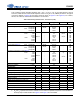
1 PIN DESCRIPTION
Pin Name # Pin Description
VLC
5
Control Interface Power (Input) - Positive power for the hardware/software control interface
VD_FILT
6
Regulator Voltage (Output) - Filter connection for internal voltage regulator
GND
7, 19
Ground (Input) - Ground reference
RMCK
8
Recovered Master Clock (Output) - Outputs a master clock derived from LRCK
VLS
9
Serial Audio Interface Power (Input) - Positive power for the serial audio interface
SCLK
10
Serial Clock (Input) - Serial bit-clock for the serial audio interface
SDIN
11
Serial Audio Data Input (Input) - Input for two’s complement serial audio data
LRCK
12
Left/Right Clock (Input) - Determines which channel, Left or Right, is currently active on the serial
audio data line
TSTO 13 Test Output - These pins need to be floating and not connected to any trace or plane.
AOUTA+,-
AOUTB+,-
14, 15,
22, 23
Differential Analog Outputs (Output) - The full scale differential output level is specified in “DAC Ana-
log Characteristics - Commercial (-CZZ)” on page 8.
AMUTEC
BMUTEC
16, 21 Mute Control (Output) - Control signals for optional mute circuit.
VBIAS
17
Positive Voltage Reference (Output) - Positive reference voltage for the internal DAC
VA
18
Analog Power (Input) - Positive power supply for the analog section
VQ
20
Quiescent Voltage (Output) - Filter connection for internal quiescent voltage
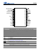
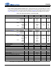
DIF2(AD1/CDOUT) RST
DEM(AD0/CS)AOUTB-
DIF0(SDA/CDIN) AOUTB+
DIF1(SCL/CCLK) BMUTEC
VLC VQ
VD_FILT GND
GND VA
RMCK VBIAS+
VLS AMUTEC
SCLK AOUTA+
SDIN AOUTA-
LRCK TSTO
2
3
4
5
6
7
8
17
18
19
20
21
22
23
9
10
11
12
13
14
15
16
24
1