
Manual

DS691F2 25
CS4350
6.3 SPI Mode
In SPI Mode, data is clocked into the serial control data line, CDIN, by the serial control port clock, CCLK
(see Figure 20 for the clock to data relationship). There are no AD0 or AD1 pins. Pin CS
is the chip select
signal and is used to control SPI writes to the control port. When the device detects a high-to-low transition
on the AD0/CS
pin after power-up, SPI Mode will be selected. All signals are inputs and data is clocked in
on the rising edge of CCLK.
6.3.1 SPI Write
To write to the device, follow the procedure below while adhering to the control port switching specifica-
tions in ”Switching Characteristics - Control Port - SPI Format” on page 14.
1. Bring CS
low.
2. The address byte on the CDIN pin must then be 10011110 (R/W
=0).
3. Write to the memory address pointer, MAP. This byte points to the register to be written.
4. Write the desired data to the register pointed to by the MAP.
5. If the INCR bit (see Section 6.1) is set to 1, repeat the previous step until all the desired registers are
written, then bring CS
high.
6. If the INCR bit is set to 0 and further SPI writes to other registers are desired, it is necessary to bring
CS
high, and follow the procedure detailed from step 1. If no further writes to other registers are
desired, bring CS
high
6.3.2 SPI Read
To read from the device, follow the procedure below while adhering to the values specified in ”Switching
Characteristics - Control Port - SPI Format” on page 14.
1. Bring CS
low.
2. The address byte on the CDIN pin must then be 10011111 (R/W
=1).
3. CDOUT pin will then output the data from the register pointed to by the MAP, which is set during the
SPI write operation.
4. If the INCR bit (see Section 6.1) is set to 1, keep CS
low and continue providing clocks on CCLK to
read from multiple consecutive registers. Bring CS
high when reading is complete.
5. If the INCR bit is set to 0 and further SPI reads from other registers are desired, it is necessary to bring
CS
high, and follow the procedure detailed from step 1. If no further reads from other registers are
desired, bring CS
high.
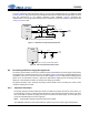
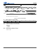
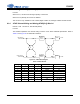
4 5 6 7 24 25
SCL
CHIP ADDRESS MAP BYTE DATA
DATA +1
START
ACK
STOP
ACKACKACK
1 0 0 1 0 AD1 AD0 R/W
SDA
6 5 4 3 2 1 0
7 6 1 0 7 6 1 0 7 6 1 0
0 1 2 3 8 9 12 16 17 18 19 10 11 13 14 15 27 28
26
DATA +n
INC
Figure 19. Control Port Timing, I²C Mode