
Manual

DS691F2 23
CS4350
5 STAND-ALONE OPERATION
5.1 Serial Port Format Selection
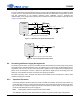
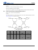
The desired serial audio format is selected with the DIF2, DIF1 and DIF0 pins. For an explanation of the
required relationship between the LRCK, SCLK and SDIN, see Figures 11-13. For all formats, SDIN is valid
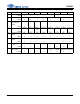
on the rising edge of SCLK. TDM Mode requires the selection of which stereo pair time “slot” is used to out-
put data as shown in Table 12 and Figure 15.
Note: The group delay for TDM slot 0 channel B differs from the group delay of all other interface formats
and TDM slots/channels by one sample. Refer to the group delay specification in the combined in-
terpolation and on-chip analog filter response specifications table.
5.2 De-Emphasis Control
When pulled to VLC, the DEM pin activates the 44.1 kHz de-emphasis filter. When pulled to GND, the DEM
pin turns off the de-emphasis filter.
5.3 Popguard
Transient Control
In Stand-Alone Mode, Popguard is selected by placing a 47 k resistor between RMCK and VLS. Popguard
is defeated in Stand-Alone Mode by placing a 47 k resistor between RMCK and ground.
6 CONTROL PORT OPERATION
The control port is used to load all the internal register settings (see ”Register Description” on page 28). The oper-
ation of the control port may be completely asynchronous with the audio sample rate. However, to avoid potential
interference problems, the control port pins should remain static if no operation is required.
The control port can operate in I²C or SPI mode.
6.1 MAP Auto Increment
The device has a MAP (memory address pointer) auto-increment capability enabled by the INCR bit (also
the MSB) of the MAP. If INCR is set to 0, MAP will stay constant for consecutive writes or reads. If INCR is
set to 1, MAP will auto increment after each byte is read or written, allowing block reads or writes of con-
secutive registers.
6.2 I²C Mode
In the I²C Mode, data is clocked into and out of the bi-directional serial control data line, SDA, by the serial
control port clock, SCL (see Figure 19 for the clock to data relationship). There is no CS
pin. AD1 and AD0
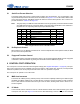
DIF2 DIF1 DIF0 DESCRIPTION FORMAT FIGURE
000
Left-Justified, up to 24-bit data
0 12
001
I²S, up to 24-bit data
1 11
010
Right-Justified, 16-bit data
2 13
011
Right-Justified, 24-bit data
3 13
100
TDM slot 0
4 15
101
TDM slot 1
5 15
110
TDM slot 2
6 15
111
TDM slot 3
7 15
Table 12. Digital Interface Format - Stand-Alone Mode