
Manual

10 DS691F2
CS4350
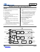
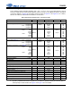
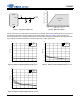
Figures 3 through 5 show typical THD+N performance for CS4350 devices that exhibit the maximum full scale out-
put voltages as specified in the DAC Analog Characteristics tables (see page 8 and 9). With decreasing VA,
THD+N performance is increasingly affected by the full scale output voltage and temperature, with higher full scale
output voltage and lower temperatures corresponding to lower THD+N performance.
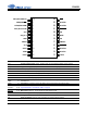
AOUTx
3.3 µF
Analog
Output
+
CS4350
GND
R
L
C
L
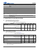
100
50
75
25
2.5
51015
Safe Operating
Region
Capacitive Load -- C (pF)
L
Resistive Load -- R (k
)
L
125
3
20
Figure 1. Equivalent Output Load Figure 2. Maximum Loading
-3-2.5-2-1.5-1-0.50
-100
-90
-80
-70
-60
-50
-40
-30
Output Amplitude(dB)
THD+N (dB)
TA = -40° C
TA = 25° C
TA = 85° C
-3-2.5-2-1.5-1-0.50
-100
-90
-80
-70
-60
-50
-40
-30
Output Amplitude(dB)
THD+N (dB)
TA = -40° C
TA = 25° C
TA = 85° C
Figure 3. THD+N vs Output Amplitude for VA = 5.0 V Figure 4. THD+N vs Output Amplitude for VA = 3.3 V
-3-2.5-2-1.5-1-0.50
-100
-90
-80
-70
-60
-50
-40
-30
Output Amplitude(dB)
THD+N (dB)
TA = -40° C
TA = 25° C
TA = 85° C
Figure 5. THD+N vs Output Amplitude for VA = 3.14 V