CS4350 192-kHz Stereo DAC with Integrated PLL Features Advanced multibit delta-sigma architecture 109 dB dynamic range -91 dB THD+N Popguard® technology for control of clicks and pops Hardware popguard disable for fast startups Supports all standard serial audio formats 24-bit conversion including time-division multiplexed (TDM) Supports audio sample rates up to 192 kHz +1.5- to 5.0-V logic supplies for serial port Low-latency digital filtering +3.3- to 5.
CS4350 Description The CS4350 is a complete stereo digital-to-analog system including PLL-based master clock derivation, digital interpolation, 5th-order multibit delta-sigma digital-to-analog conversion, digital de-emphasis, volume control, channel mixing, and analog filtering.
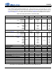
CS4350 TABLE OF CONTENTS 1 PIN DESCRIPTION................................................................................................................................... 6 2 CHARACTERISTICS AND SPECIFICATIONS........................................................................................ 7 2.1 Recommended Operating Conditions ............................................................................................. 7 2.2 Absolute Maximum Ratings ...............................................
CS4350 8.2.2 De-Emphasis Control (DEM[1:0]) Bits 3-2 ........................................................................... 29 8.2.3 Functional Mode (FM[1:0]) Bits 1-0...................................................................................... 29 8.3 Volume Mixing and Inversion Control - Register 03h .................................................................... 29 8.3.1 Channel A Volume = Channel B Volume (VOLB=A) Bit 7 ................................................... 29 8.3.
CS4350 LIST OF FIGURES Figure 1. Equivalent Output Load .............................................................................................................. 10 Figure 2. Maximum Loading....................................................................................................................... 10 Figure 3. THD+N vs Output Amplitude for VA = 5.0 V ............................................................................... 10 Figure 4. THD+N vs Output Amplitude for VA = 3.3 V .........
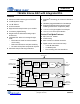
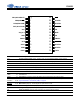
CS4350 1 PIN DESCRIPTION DIF2(AD1/CDOUT) 1 24 RST DEM(AD0/CS) 2 23 AOUTB- DIF0(SDA/CDIN) 3 22 AOUTB+ DIF1(SCL/CCLK) 4 21 BMUTEC VLC 5 20 VQ VD_FILT 6 19 GND GND 7 18 VA RMCK 8 17 VBIAS+ 16 AMUTEC SCLK 9 10 15 AOUTA+ SDIN 11 14 AOUTA- LRCK 12 13 TSTO VLS Pin Name # Pin Description VLC 5 Control Interface Power (Input) - Positive power for the hardware/software control interface VD_FILT 6 Regulator Voltage (Output) - Filter connection for internal voltag
CS4350 Pin Name # Pin Description RST 24 Reset (Input) - When pulled low, device will power down and reset all internal registers to their default settings. Control Port Definitions AD1/CDOUT 1 Address Bit 1/Serial Control Data Out (I/O) - Chip address bit 1 in I²C Mode or data output in SPI Mode AD0/CS 2 Address Bit 0/Chip Select (Input) - Chip address bit 0 in I²C Mode or Chip Select in SPI Mode SDA/CDIN 3 Serial Control Data In (I/O) - Input/Output for I²C data.
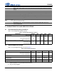
CS4350 2.3 DAC Analog Characteristics - Commercial (-CZZ) Test conditions (unless otherwise specified): VLS = VLC = 3.3 V; TA = 25° C; Input test signal is a 997 Hz sine wave; Valid with the recommended capacitor values on VD_FILT, VQ, VBIAS (as shown in the typical connection diagram in Figure 10) and output circuits as shown in Figure 17 and Figure 18; Fs = 48 kHz, 96 kHz, and 192 kHz; measurement bandwidth 10 Hz to 20 kHz. Table 3.
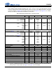
CS4350 2.4 DAC Analog Characteristics - Automotive (-DZZ) Test conditions (unless otherwise specified): VLS = 1.35 V to 5.25 V, VLC = 3.14 V to 5.25 V, TA = -40° C to 105° C, input test signal is a 997 Hz sine wave; Valid with the recommended capacitor values on VFILT, VQ, VBIAS (as shown in the typical connection diagram in Figure 10) and output circuits as shown in Figure 17 and Figure 18; Fs = 48 kHz, 96 kHz, and 192 kHz; Measurement bandwidth 10 Hz to 20 kHz. Table 4.
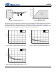
CS4350 Capacitive Load -- C L (pF) 125 CS4350 AOUTx 3.3 µF + Analog Output RL CL 100 75 Safe Operating Region 50 25 GND 2.5 3 Figure 1. Equivalent Output Load 5 10 15 20 Resistive Load -- RL (k ) Figure 2. Maximum Loading Figures 3 through 5 show typical THD+N performance for CS4350 devices that exhibit the maximum full scale output voltages as specified in the DAC Analog Characteristics tables (see page 8 and 9).
CS4350 2.5 Combined Interpolation and On-Chip Analog Filter Response The filter characteristics have been normalized to the sample rate (Fs) and is referenced to the desired sample rate by multiplying the given characteristic by Fs. Amplitude vs. Frequency plots of this data are available in the “Filter Plots” on page 35. Table 5. Combined Interpolation and On-Chip Analog Filter Response Parameter Min Typ Max Unit 0 - .454 Fs Fast Roll-Off Passband (Note 6) -0.01 dB corner (Single Speed) -0.
CS4350 2.6 Switching Specifications - Serial Audio Interface Inputs: Logic 0 = GND; Logic 1 = VLS; CL = 20 pF. Table 6. Switching Specifications - Serial Audio Interface Parameters Symbol Min Max Units 7.680 55.3 MHz 45 55 % 3.14 V VA 5.25 V and 1.35 V VLS 5.
CS4350 tlrckh LRCK (input) tlckd tlcks LRCK tsckl tsckh (Input) tfsh tfss tsckh tsckl SCLK SCLK (input) (Input) tds tdh SDIN tds MSB (input) SDIN MSB-1 MSB (Input) Figure 6. Serial Port Timing, Non-TDM Mode 2.7 tdh MSB-1 Figure 7. Serial Port Timing, TDM Mode Switching Characteristics - Control Port - I²C Format Inputs: Logic 0 = GND; Logic 1 = VLC; CL = 20 pF. Table 7.
CS4350 2.8 Switching Characteristics - Control Port - SPI Format Inputs: Logic 0 = GND; Logic 1 = VLC; CL = 20 pF. Table 8. Switching Characteristics - Control Port - SPI Format Parameter Symbol Min Max Unit CCLK Clock Frequency fsclk - 6 MHz RST Rising Edge to CS Falling tsrs 500 - ns CCLK Edge to CS Falling (Note 12) tspi 500 - ns CS High Time Between Transmissions tcsh 1.
CS4350 2.9 Digital Characteristics Table 9. Digital Characteristics Parameters High-Level Input Voltage Symbol Min Typ Max Units VLC or VLS = 3.3 V VIH VIH 0.7•VL 2.0 - - V V VLS = 2.5 V VIH 1.7 - - V VLS = 1.5 V VLC or VLS = 5.0 V VIH 0.75•VL - - V VLC or VLS = 3.3 V VIL VIL - - 0.35•VL 0.8 V V VLS = 2.5 V VIL - - 0.7 V VLS = 1.5 V VIL - - 0.25•VL V Iin 8 - ±10 - A pF V VLC or VLS = 5.
CS4350 3 TYPICAL CONNECTION DIAGRAM +3.3 V or +5 V + 0.1 µF 18 + 10 µF VA VLS = PopGuard Enable GND = PopGuard Disable 10 µF VBIAS+ 17 47 k 8 RMCK Digital Audio Source 12 LRCK VD_FILT 6 10 SCLK 0.1 µF + 10 µF 11 SDIN +1.5 V to +5 V 9 VLS AMUTEC 16 0.1 µF AOUTA+ 15 CS4350 AOUTA- 14 Differential or Singleended Output Filter AOUTA Differential or Singleended Output Filter AOUTB 5 VLC +3.3 V to +5 V 0.
CS4350 4 APPLICATIONS 4.1 Sample Rate Range and Oversampling Mode Detect The device operates in one of three oversampling modes based on the input sample rate. In Control Port Mode, the allowed sample rate range in each mode will depend on how the FM[1:0] bits are configured. In Stand-Alone Mode, the sample rate range will be according to Table 11. 4.1.1 Sample Rate Auto-Detect The Auto-Detect feature is enabled by default.
CS4350 4.3 Digital Interface Format The device will accept audio samples in 1 of 8 digital interface formats, as shown in Table 12 on page 23 for Stand-Alone Mode and Table 13 on page 28 for Control Port Mode. The desired serial audio interface format is selected via the DIF[2:0] bits in Control Port Mode (see Section 8.2.1), or the DIF[2:0] pins in Stand-Alone Mode (see Section 5.1). For illustrations of the required relationship between LRCK, SCLK and SDIN, see Figures 11-13.
CS4350 4.3.1 Time-Division Multiplex (TDM) Mode Four TDM interface modes are available that allow the CS4350 to input stereo PCM data in one of 4 time “slots”. Figure 14 shows the serial port connections necessary to input 8-channel TDM data into four CS4350 devices, and the corresponding DIF[2:0] pin or register-bit settings required for each CS4350. Figure 15 shows the TDM data format for each of the four CS4350 devices shown in Figure 14.
CS4350 4.4 De-Emphasis The device includes on-chip digital de-emphasis. Figure 16 shows the de-emphasis curve for Fs equal to 44.1 kHz. The frequency response of the de-emphasis curve will scale proportionally with changes in sample rate, Fs. Gain dB T1=50 µs 0dB T2 = 15 µs -10dB F1 3.183 kHz F2 Frequency 10.61 kHz Figure 16. De-Emphasis Curve Note: 4.5 De-emphasis is only available in Single-Speed Mode.
CS4350 4.6.2 Control Port Mode 1. Hold RST low until the power supply is stable and the left/right clock is fixed to the appropriate frequency, as discussed in Section 4.2. In this state, the control port is reset to its default settings, VQ will remain low, and VBIAS will be connected to VA. 2. Bring RST high. The device will remain in a low-power state with VQ low. 3.
CS4350 4.8 Analog Output and Filtering The Cirrus Application Note titled Design Notes for a 2-Pole Filter with Differential Input, available as AN48 at www.cirrus.com, discusses the second-order Butterworth filter and differential-to-single-ended converter that was implemented on the CS4350 evaluation board, CDB4350. Figure 17 illustrates this implementation. If only single-ended outputs from the CS4350 are required, the passive output filter shown in Figure 18 can be used. 5600 pF CS4350 4.
CS4350 5 STAND-ALONE OPERATION 5.1 Serial Port Format Selection The desired serial audio format is selected with the DIF2, DIF1 and DIF0 pins. For an explanation of the required relationship between the LRCK, SCLK and SDIN, see Figures 11-13. For all formats, SDIN is valid on the rising edge of SCLK. TDM Mode requires the selection of which stereo pair time “slot” is used to output data as shown in Table 12 and Figure 15.
CS4350 enable the user to alter the chip address (10010[AD1][AD0][R/W]) and should be tied to VLC or GND as required before powering up the device. SPI Mode will be selected if the device ever detects a high to low transition on the AD0/CS pin after power-up. 6.2.1 I²C Write To write to the device, follow the procedure below while adhering to the control port Switching Specifications in ”Switching Characteristics - Control Port - I²C Format” on page 13. 1.
CS4350 0 1 2 3 4 5 6 7 8 9 10 11 12 13 14 15 16 17 18 19 24 25 26 27 28 SCL CHIP ADDRESS 1 0 0 1 0 AD1 AD0 R/W SDA MAP BYTE INC 6 ACK 5 4 3 DATA +1 DATA 2 1 0 7 6 1 ACK 0 7 6 1 DATA +n 0 7 6 1 ACK 0 ACK STOP START Figure 19. Control Port Timing, I²C Mode 6.3 SPI Mode In SPI Mode, data is clocked into the serial control data line, CDIN, by the serial control port clock, CCLK (see Figure 20 for the clock to data relationship). There are no AD0 or AD1 pins.
CS4350 CS CCLK C H IP ADDRESS CDIN MAP 1001111 C H IP ADDRESS DATA LSB MSB R/W b y te 1 1001111 R/W b y te n High Impedance CDOUT MSB LSB MSB LSB MAP = Memory Address Pointer, 8 bits, MSB first Figure 20. Control Port Timing, SPI Mode 6.4 Memory Address Pointer (MAP) 7 INCR 0 6.4.1 6 Reserved 0 5 Reserved 0 4 Reserved 0 3 MAP3 0 2 MAP2 0 1 MAP1 0 0 MAP0 0 INCR (Auto Map Increment Enable) Default = ‘0’ 0 - Disabled 1 - Enabled 6.4.
CS4350 7 REGISTER QUICK REFERENCE Addr Function 7 6 5 4 1h Device and RevID DeviceID4 DeviceID3 DeviceID2 DeviceID1 2h Mode Control 3h Volume, Mixing, and Inversion Control default default default 4h Mute Control default 5h Channel A Volume Control 6h Channel B Volume Control 7h Ramp and Filter Control default default default 8h Misc.
CS4350 8 REGISTER DESCRIPTION Note: All register access is Read/Write unless specified otherwise 8.1 Device and Revision ID - Register 01h 7 Device4 1 6 Device3 1 5 Device2 1 4 Device1 1 3 Device0 - 2 Rev2 - 1 Rev1 - 0 Rev0 - 1 FM1 0 0 FM0 0 Function: This register is Read-Only. It is decoded as follows: 8.2 Rev Register 01h contents A 1111,0000 B 1111,0001 C2 1111,1111 Mode Control - Register 02h 7 Reserved 0 8.2.
CS4350 8.2.2 De-Emphasis Control (DEM[1:0]) Bits 3-2 Default = 0 00 - No De-emphasis 01 - 44.1 kHz De-emphasis 10 - 48 kHz De-emphasis 11 - 32 kHz De-emphasis Gain dB T1=50 µs 0dB T2 = 15 µs Function: -10dB Selects the appropriate digital filter to maintain the standard 15 s/50 s digital de-emphasis filter response at 32, 44.1 or 48 kHz sample rates. (See Figure 21) Note: 8.2.3 F1 3.183 kHz F2 Frequency 10.61 kHz Figure 21.
CS4350 8.3.3 Invert Signal Polarity (INVERT_B) Bit 5 Function: When set to 1, this bit inverts the signal polarity of channel B. When set to 0 (default), this function is disabled. This function is only available for Left Justified, Right Justified 16, and Right Justified 24 data formats. 8.3.4 ATAPI Channel Mixing and Muting (ATAPI[3:0]) Bits 3-0 Default = 1001 - AOUTA=aL, AOUTB=bR (Stereo) Function: The CS4350 implements the channel mixing functions of the ATAPI CD-ROM specification.
CS4350 Table 14. ATAPI Decode (Continued) ATAPI_A1 ATAPI_A0 ATAPI_B1 ATAPI_B0 8.4 AOUTA AOUTB 1 0 0 0 aL MUTE 1 0 0 1 aL bR 1 0 1 0 aL bL 1 0 1 1 aL b[(L+R)/2] 1 1 0 0 a[(L+R)/2] MUTE 1 1 0 1 a[(L+R)/2] bR 1 1 1 0 a[(L+R)/2] bL 1 1 1 1 a[(L+R)/2] b[(L+R)/2] Mute Control - Register 04h 7 AMUTE 1 8.4.
CS4350 8.5 Channel A & B Volume Control - Register 05h & 06h 7 VOL7 0 6 VOL6 0 5 VOL5 0 4 VOL4 0 3 VOL3 0 2 VOL2 0 1 VOL1 0 0 VOL0 0 Digital Volume Control (VOL[7:0]) Bits 7-0 Default = 00h (0 dB) Function: The Digital Volume Control registers allow independent control of the signal levels in 1/2 dB increments from 0 to -127.5 dB. Volume settings are decoded as shown in Table 15. The volume changes are implemented as dictated by the Soft and Zero Cross bits in the Power and Muting Control register.
CS4350 Soft Ramp and Zero Cross Soft Ramp and Zero Cross Enable dictate that signal level changes, either by attenuation changes or muting, will occur in 1/8 dB steps and be implemented on a signal zero crossing. The 1/8 dB level change will occur after a time-out period between 512 and 1024 sample periods (10.7 ms to 21.3 ms at 48 kHz sample rate) if the signal does not encounter a zero crossing. The zero cross function is independently monitored and implemented for each channel. 8.6.
CS4350 8.7.2 Freeze Controls (FREEZE) Bit 5 Function: When set to 1, this function allows modifications to be made to the registers without the changes taking effect until FREEZE is set back to 0. To make multiple changes in the Control Port registers take effect simultaneously, enable the FREEZE bit, make all register changes, then disable the FREEZE bit. When set to 0 (default), register changes take effect immediately. 8.7.
CS4350 9 FILTER PLOTS 0 20 20 40 40 Amplitude (dB) Amplitude (dB) 0 60 60 80 80 100 100 120 0.4 0.5 0.6 0.7 0.8 Frequency(normalized to Fs) 0.9 120 1 0.4 0.5 0.6 0.7 0.8 Frequency(normalized to Fs) 0.9 1 0.02 0.02 0.015 0.015 0.01 0.01 0.005 0.005 Amplitude (dB) Figure 24. Stopband Rejection (slow), all Modes Amplitude (dB) Figure 23. Stopband Rejection (fast), all Modes 0 0 0.005 0.005 0.01 0.01 0.015 0.015 0.02 0 0.05 0.1 0.15 0.2 0.25 0.
0.5 0.5 0.4 0.4 0.3 0.3 0.2 0.2 0.1 0.1 Amplitude (dB) Amplitude (dB) CS4350 0 −0.1 0 −0.1 −0.2 −0.2 −0.3 −0.3 −0.4 −0.4 −0.5 0 0.05 0.1 0.15 0.2 Frequency (normalized to Fs) 0.25 0.3 −0.5 Figure 29. Quad-Speed (fast) Passband Detail 0 0.05 0.1 0.15 0.2 Frequency (normalized to Fs) 0.25 0.3 Figure 30.
CS4350 11 PACKAGE DIMENSIONS 24L TSSOP (4.4 mm BODY) PACKAGE DRAWING N D E11 A2 E A e b2 A1 SIDE VIEW END VIEW L SEATING PLANE 1 2 3 TOP VIEW DIM MIN INCHES NOM A A1 A2 b D E E1 e L µ -0.002 0.03346 0.00748 0.303 0.248 0.169 -0.020 0° -0.004 0.0354 0.0096 0.307 0.2519 0.1732 0.026 BSC 0.024 4° MAX 0.043 0.006 0.037 0.012 0.311 0.256 0.177 -0.028 8° MIN MILLIMETERS NOM NOTE MAX -0.05 0.85 0.19 7.70 6.30 4.30 -0.50 0° --0.90 0.245 7.80 6.40 4.40 0.65 BSC 0.60 4° 1.10 0.15 0.95 0.
CS4350 13 ORDERING INFORMATION Product CS4350 CDB4350 Description 192 kHz Stereo DAC with Integrated PLL Package Pb-Free Grade Temp Range Commercial -40° to +85°C 24-TSSOP Evaluation Board for CS4350 YES Automotive -40° to +105°C - - Container Order# Rail CS4350-CZZ Tape and Reel CS4350-CZZR Rail CS4350-DZZ Tape and Reel CS4350-DZZR - CDB4350 - 14 REVISION HISTORY Release Changes F1 • • • • • Updated “DAC Analog Characteristics - Commercial (-CZZ)” on page 8.