
Manual

CS4341A
4 DS582F2
LIST OF FIGURES
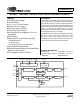
Figure 1. Typical Connection Diagram .......................................................................................... 6
Figure 2. I
2
S Data .......................................................................................................................... 8
Figure 3. Left Justified up to 24-Bit Data ....................................................................................... 9
Figure 4. Right Justified Data ........................................................................................................ 9
Figure 5. De-Emphasis Curve ....................................................................................................... 9
Figure 6. I
2
C Buffer Example ...................................................................................................... 11
Figure 7. Control Port Timing, I2C Mode ..................................................................................... 13
Figure 8. Control Port Timing, SPI mode .................................................................................... 14
Figure 9. ATAPI Block Diagram .................................................................................................. 21
Figure 10. Output Test Load ......................................................................................................... 25
Figure 11. Maximum Loading ........................................................................................................ 25
Figure 12. Single-Speed Stopband Rejection ............................................................................... 27
Figure 13. Single-Speed Transition Band ..................................................................................... 27
Figure 14. Single-Speed Transition Band (Detail) ......................................................................... 27
Figure 15. Single-Speed Passband Ripple ................................................................................... 27
Figure 16. Double-Speed Stopband Rejection .............................................................................. 27
Figure 17. Double-Speed Transition Band .................................................................................... 27
Figure 18. Double-Speed Transition Band (Detail) ....................................................................... 28
Figure 19. Double-Speed Passband Ripple .................................................................................. 28
Figure 20. Serial Input Timing ....................................................................................................... 29
Figure 21. Control Port Timing - I
2
C Mode .................................................................................... 30
Figure 22. Control Port Timing - SPI Mode ................................................................................... 31
LIST OF TABLES
Table 1. CS4341A Auto-Detect .......................................................................................................... 7
Table 2. CS4341A Mode Select ......................................................................................................... 7
Table 3. Single-Speed Mode Standard Frequencies.......................................................................... 8
Table 4. Double-Speed Mode Standard Frequencies ........................................................................ 8
Table 5. Quad-Speed Mode Standard Frequencies........................................................................... 8
Table 6. Digital Interface Format ...................................................................................................... 18
Table 7. ATAPI Decode.................................................................................................................... 20
Table 8. Example Digital Volume Settings ....................................................................................... 22