
User guide

CS4341
DS298F5 3
8.1 SOIC ..............................................................................................................................................32
8.2 TSSOP ..........................................................................................................................................33
9. PACKAGE THERMAL RESISTANCE .................................................................................................33
10. REFERENCES ....................................................................................................................................34
11. REVISION HISTORY ..........................................................................................................................34
LIST OF FIGURES
Figure 1. Output Test Load .........................................................................................................................6
Figure 2. Maximum Loading ........................................................................................................................6
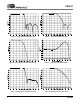
Figure 3. Single-Speed Stopband Rejection ...............................................................................................8
Figure 4. Single-Speed Transition Band .....................................................................................................8
Figure 5. Single-Speed Transition Band (Detail) .........................................................................................8
Figure 6. Single-Speed Passband Ripple ...................................................................................................8
Figure 7. Double-Speed Stopband Rejection ..............................................................................................8
Figure 8. Double-Speed Transition Band ....................................................................................................8
Figure 9. Double-Speed Transition Band (Detail) .......................................................................................9
Figure 10. Double-Speed Passband Ripple ..................................................................................................9
Figure 11. Serial Input Timing (External SCLK) ..........................................................................................10
Figure 12. Internal Serial Mode Input Timing ..............................................................................................11
Figure 13. Internal Serial Clock Generation ................................................................................................11
Figure 14. Control Port Timing - I²C Mode ..................................................................................................12
Figure 15. Control Port Timing - SPI Mode .................................................................................................13
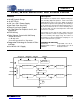
Figure 16. Typical Connection Diagram ......................................................................................................16
Figure 17. CS4341 Formats 0-1 - I²S up to 24-Bit Data ..............................................................................18
Figure 18. CS4341 Format 2 - Left Justified up to 24-Bit Data ...................................................................18
Figure 19. CS4341 Formats 3-6 - Right Justified ........................................................................................18
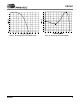
Figure 20. De-Emphasis Curve ...................................................................................................................19
Figure 21. I²C Buffer Example .....................................................................................................................21
Figure 22. I²C Write .....................................................................................................................................22
Figure 23. I²C Read .....................................................................................................................................23
Figure 24. Control Port Timing, SPI Mode ..................................................................................................23
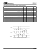
Figure 25. ATAPI Block Diagram ................................................................................................................29
LIST OF TABLES
Table 1. CS4341 Speed Modes .....................................................................................................................17
Table 2. Single-Speed Mode Standard Frequencies .....................................................................................17
Table 3. Double-Speed Mode Standard Frequencies....................................................................................17
Table 4. Internal SCLK/LRCK Ratio...............................................................................................................18
Table 5. Digital Interface Format....................................................................................................................26
Table 6. ATAPI Decode..................................................................................................................................28
Table 7. Example Digital Volume Settings .....................................................................................................30