
User guide

CS4341
DS298F5 23
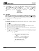
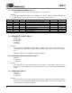
4.9.4 SPI Mode
In SPI mode, data is clocked into the serial control data line, CDIN, by the serial control port clock,
CCLK (see Figure 24 for the clock to data relationship). There is no AD0 pin. Pin CS
is the chip
select signal and is used to control SPI writes to the control port. When the device detects a high
to low transition on the AD0/CS
pin after power-up, SPI mode will be selected. All signals are inputs
and data is clocked in on the rising edge of CCLK.
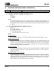
4.9.4a SPI Write
To write to the device, follow the procedure below while adhering to the control port Switching
Specifications in section 1.
1) Bring CS
low.
2) The address byte on the CDIN pin must then be 00100000.
3) Write to the memory address pointer, MAP. This byte points to the register to be written.
4) Write the desired data to the register pointed to by the MAP.
5) If the INCR bit (see section 4.9.2a) is set to 1, repeat the previous step until all the desired
registers are written, then bring CS
high.
6) If the INCR bit is set to 0 and further SPI writes to other registers are desired, it is necessary
to bring CS
high, and repeat the procedure detailed from step 1. If no further writes to other
registers are desired, bring CS
high.
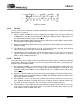
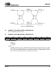
SDA
SCL
001000 AD0 W
Start
ACK
MAP
1-8
ACK
001000 AD0 R
Repeated START
or
Aborted WRITE
ACK
Data 1-8
(pointed to by MAP)
Data 1-8
(pointed to by MAP)
ACK
Stop
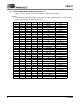
Figure 23. I²C Read
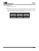
MAP
MSB
LSB
DATA
byte 1
byte n
R/W
MAP = Memory Address Pointer
ADDRESS
CHIP
CDIN
CCLK
CS
0010000
Figure 24. Control Port Timing, SPI Mode