
User guide

CS4341
DS298F5 21
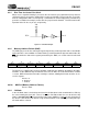
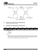
4.9.1 Rise Time for Control Port Clock
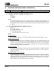
When excess capacitive loading is present on the I²C clock line, pin 6 (SCL/CCLK) may not have
sufficient hysteresis to meet the standard I²C rise time specification. This prevents the use of com-
mon I²C configurations with a resistor pull-up. A workaround is achieved by placing a Schmitt Trig-
ger buffer, a 74HC14 for example, on the SCL line just prior to the CS4341. This will not affect the
operation of the I²C bus as pin 6 is an input only.
4.9.2 Memory Address Pointer (MAP)
The MAP byte precedes the control port register byte during a write operation and is not available
again until after a start condition is initiated. During a read operation the byte transmitted after the
ACK
will contain the data of the register pointed to by the MAP (see section 4.9.3 for write/read
details).
4.9.2a INCR (Auto Map Increment)
The device has a MAP auto increment capability enabled by the INCR bit (the MSB) of the MAP.
If INCR is set to 0, MAP will stay constant for successive I²C writes or reads and SPI writes. If INCR
is set to 1, MAP will auto increment after each byte is written, allowing block reads or writes of suc-
cessive registers.
Default = ‘0’
0 - Disabled
1 - Enabled
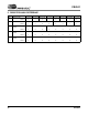
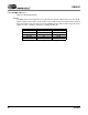
4.9.2b MAP0-3 (Memory Address Pointer)
Default = ‘0000’
4.9.3 I²C Mode
In the I²C Mode, data is clocked into and out of the bi-directional serial control data line, SDA, by
the serial control port clock, SCL. There is no CS
pin. Pin AD0 enables the user to alter the chip
address (001000[AD0][R/W
]) and should be tied to VA or AGND as required, before powering up
the device. If the device ever detects a high to low transition on the AD0/CS
pin after power-up,
SPI mode will be selected.
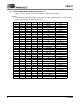
76543210
INCR Reserved Reserved Reserved MAP3 MAP2 MAP1 MAP0
00000000
Pin 6
VA
SCL
Figure 21. I²C Buffer Example