
User guide

CS4341
DS298F5 15
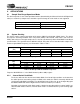
2. PIN DESCRIPTION
Pin Name # Pin Description
RST
1
Reset (Input) - Powers down device and resets registers to their default settings.
SDATA
2
Serial Audio Data (Input) - Input for two’s complement serial audio data.
SCLK
3
Serial Clock (Input) -Serial clock for the serial audio interface.
LRCK
4
Left Right Clock (Input) - Determines which channel, Left or Right, is currently active on the
serial audio data line.
MCLK
5
Master Clock (Input) - Clock source for the delta-sigma modulator and digital filters.
SCL/CCLK
6
Serial Control Port Clock (Input) - Serial clock for the control port interface.
SDA/CDIN
7 Serial Control Data I/O (Input/Output) - Input/Output for I²C data. Input for SPI data.
AD0/CS
8
Address Bit / Chip Select (Input) - Chip address bit in I²C Mode. Control signal used to select
the chip in SPI mode.
FILT+
9
Positive Voltage Reference (Output) - Positive voltage reference for the internal
sampling circuits.
VQ
10
Quiescent Voltage (Output) - Filter connection for internal quiescent reference voltage.
REF_GND
11
Reference Ground (Input) - Ground reference for the internal sampling circuits.
AOUTB
AOUTA
12
15
Analog Outputs (Output) - The full-scale analog output level is specified in the
Analog Characteristics table.
AGND
13
Analog Ground (Input)
VA
14 Power (Input) - Positive power for the analog, digital, and serial audio interface sections.
MUTEC
16
Mute Control (Output) - Control signal for an optional mute circuit.
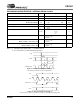
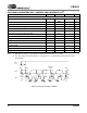
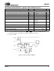
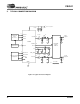
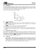
152
143
134
161
116
107
98
125
RST MUTEC
SDATA AOUTA
SCLK VA
LRCK AGND
MCLK AOUTB
SCL/CCLK REF_GND
SDA/CDIN VQ
AD0/CS
FILT+