CS4341 24-Bit, 96 kHz Stereo DAC with Volume Control Features Description ! 101 The CS4341 is a complete stereo digital-to-analog system including digital interpolation, fourth-order DeltaSigma digital-to-analog conversion, digital de-emphasis and switched capacitor analog filtering. The advantages of this architecture include: ideal differential linearity, no distortion mechanisms due to resistor matching errors, no linearity drift over time and temperature and a high tolerance to clock jitter.
CS4341 TABLE OF CONTENTS 1. CHARACTERISTICS AND SPECIFICATIONS ..................................................................................... 4 SPECIFIED OPERATING CONDITIONS .............................................................................................. 4 ABSOLUTE MAXIMUM RATINGS ........................................................................................................ 4 ANALOG CHARACTERISTICS (CS4341-KS/CZZ)...............................................................
CS4341 8.1 SOIC ..............................................................................................................................................32 8.2 TSSOP ..........................................................................................................................................33 9. PACKAGE THERMAL RESISTANCE .................................................................................................33 10. REFERENCES .......................................................
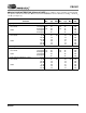
CS4341 1. CHARACTERISTICS AND SPECIFICATIONS (Min/Max performance characteristics and specifications are guaranteed over the Specified Operating Conditions. Typical performance characteristics are derived from measurements taken at TA = 25°C.) SPECIFIED OPERATING CONDITIONS (All voltages with respect to AGND = 0 V.) Parameters Symbol Min Nom Max Units Nominal 3.3 V Nominal 5.0 V VA VA 2.7 4.75 3.3 5.0 3.6 5.
CS4341 ANALOG CHARACTERISTICS (CS4341-KS/CZZ) (Test conditions (unless otherwise specified): Input test signal is a 997 Hz sine wave at 0 dBFS; measurement bandwidth is 10 Hz to 20 kHz; test load R L = 10 kΩ, CL = 10 pF (see Figure 1).) VA = 5.0 V Parameter Single-Speed Mode Dynamic Range 18 to 24-Bit 16-Bit Total Harmonic Distortion + Noise 18 to 24-Bit 16-Bit Double-Speed Mode Dynamic Range 18 to 24-Bit 16-Bit Total Harmonic Distortion + Noise 18 to 24-Bit 16-Bit DS298F5 VA = 3.
CS4341 ANALOG CHARACTERISTICS (CS4341-KS/CZZ) Parameters Symbol (Continued) Min Typ Max Units - 100 - dB Interchannel Gain Mismatch - 0.1 - dB Gain Drift - ±100 - ppm/°C 0.6•VA 0.7•VA 0.
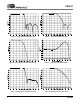
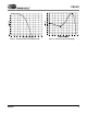
CS4341 COMBINED INTERPOLATION & ON-CHIP ANALOG FILTER RESPONSE (The filter characteristics and the X-axis of the response plots have been normalized to the sample rate (Fs) and can be referenced to the desired sample rate by multiplying the given characteristic by Fs.) Parameter Min Typ Max Unit 0 0 - 0.4535 0.4998 Fs Fs -0.02 - +0.08 dB 0.5465 - - Fs 50 - - dB Single-Speed Mode - (4 kHz to 50 kHz sample rates) Passband to -0.
CS4341 Figure 3. Single-Speed Stopband Rejection Figure 5. Single-Speed Transition Band (Detail) Figure 7. Double-Speed Stopband Rejection 8 Figure 4. Single-Speed Transition Band Figure 6. Single-Speed Passband Ripple Figure 8.
CS4341 Figure 9. Double-Speed Transition Band (Detail) DS298F5 Figure 10.
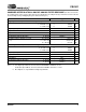
CS4341 SWITCHING SPECIFICATIONS - SERIAL AUDIO INTERFACE Parameters Min Max Units MCLK Frequency 1.024 51.
CS4341 SWITCHING CHARACTERISTICS - INTERNAL SERIAL CLOCK Parameters Min Typ Max Units MCLK Frequency 1.024 - 51.
CS4341 SWITCHING CHARACTERISTICS - CONTROL PORT INTERFACE (I²C®) Parameter Symbol Min Max Unit SCL Clock Frequency fscl - 100 kHz RST Rising Edge to Start tirs 500 - ns Bus Free Time Between Transmissions tbuf 4.7 - µs Start Condition Hold Time (prior to first clock pulse) thdst 4.0 - µs Clock Low time tlow 4.7 - µs Clock High Time thigh 4.0 - µs Setup Time for Repeated Start Condition tsust 4.
CS4341 SWITCHING CHARACTERISTICS - CONTROL PORT INTERFACE (SPI™) Parameter Symbol Min Max Unit CCLK Clock Frequency fsclk - 6 MHz RST Rising Edge to CS Falling tsrs 500 - ns tspi 500 - ns CS High Time Between Transmissions tcsh 1.
CS4341 DC ELECTRICAL CHARACTERISTICS (AGND = 0 V; all voltages with respect to AGND.) Parameters Symbol Min Typ Max Units IA IA - 15 11 18 14 mA mA - 75 33 90 42 mW mW - 60 30 - µA µA - 0.3 0.09 - mW mW - 60 40 - dB dB VQ Nominal Voltage Output Impedance Maximum allowable DC current source/sink - 0.45•VA 250 0.01 - kΩ Filt+ Nominal Voltage Output Impedance Maximum allowable DC current source/sink - VA 250 0.
CS4341 2. PIN DESCRIPTION RST 1 16 MUTEC SDATA 2 15 AOUTA SCLK 3 14 VA LRCK 4 13 AGND MCLK 5 12 AOUTB SCL/CCLK 6 11 REF_GND SDA/CDIN 7 10 VQ AD0/CS 8 9 FILT+ Pin Name # Pin Description RST 1 Reset (Input) - Powers down device and resets registers to their default settings. SDATA 2 Serial Audio Data (Input) - Input for two’s complement serial audio data. SCLK 3 Serial Clock (Input) -Serial clock for the serial audio interface.
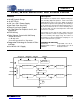
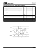
CS4341 3. TYPICAL CONNECTION DIAGRAM +3.0 V or +5.0 V + 0.1 µF 14 1 µF VA 2 Serial Audio Data Processor 3 4 SDATA 3.3 µF SCLK AOUT A 560 Ω Audio O utput A 15 + LR CK C 10 k Ω RL CS4341 M UTEC 16 External Clock 5 M CLK FILT+ VQ 6 7 Micro-Controlled Configuration O PTIO NAL MUTE CIRCUIT 9 + 10 .1 µF + 1 µF 0.1 µF 1 µF 11 SCL/CCLK REF_GND 3.3 µF SDA/CDIN 560 Ω 12 8 AO UTB AD0/CS 1 10 k Ω RST Audio O utput B + C RL AG ND 13 R L + 560 C= 4 π Fs(R L 560) Figure 16.
CS4341 4. APPLICATIONS 4.1 Sample Rate Range/Operational Mode The device operates in one of two operational modes determined by the Master Clock to Left/Right Clock ratio (see section 4.2). Sample rates outside the specified range for each mode are not supported. Input Sample Rate (Fs) 4 kHz - 50 kHz 50 kHz - 100 kHz MODE Single-Speed Mode Double-Speed Mode Table 1. CS4341 Speed Modes 4.2 System Clocking The device requires external generation of the master (MCLK) and left/right (LRCK) clocks.
CS4341 Input MCLK/LRCK Ratio 512, 256, 128 384, 192 512, 256, 128 Digital Interface Format Selection Right Justified I S up to 16 or Left Justified 24 Right Justified Bits 18, 20 or 24 Bits 16 Bits 24 Bits (Format 1) X 2 Internal SCLK/LRCK Ratio 32 X X X X 48 (Format 0) X X - 64 Table 4. Internal SCLK/LRCK Ratio 4.2.
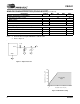
CS4341 4.4 De-Emphasis The device includes on-chip digital de-emphasis. The Mode Control (address 01h) bits select either the 32, 44.1 or 48 kHz de-emphasis filter. Figure 20 shows the de-emphasis curve for Fs equal to 44.1 kHz. The frequency response of the de-emphasis curve will scale proportionally with changes in sample rate, Fs. Please see section 6.2.3 for the desired de-emphasis control. De-emphasis is only available in Single-Speed Mode. Gain dB T1=50 µs 0dB T2 = 15 µs -10dB F1 3.
CS4341 4.6.2 Power-Down To prevent transients at power-down, the device must first enter its power-down state by enabling RST or setting the PDN bit. When this occurs, audio output ceases and the internal output buffers are disconnected from AOUTL and AOUTR. In their place, a soft-start current sink is substituted which allows the DC-blocking capacitors to slowly discharge. Once this charge is dissipated, the power to the device may be turned off and the system is ready for the next power-on. 4.6.
CS4341 4.9.1 Rise Time for Control Port Clock When excess capacitive loading is present on the I²C clock line, pin 6 (SCL/CCLK) may not have sufficient hysteresis to meet the standard I²C rise time specification. This prevents the use of common I²C configurations with a resistor pull-up. A workaround is achieved by placing a Schmitt Trigger buffer, a 74HC14 for example, on the SCL line just prior to the CS4341. This will not affect the operation of the I²C bus as pin 6 is an input only.
CS4341 SDA 001000 AD0 W ACK MAP 1-8 ACK DATA 1-8 ACK SCL Stop S tart Figure 22. I²C Write 4.9.3a I²C Write To write to the device, follow the procedure below while adhering to the control port Switching Specifications in section 6. 1) Initiate a START condition to the I²C bus followed by the address byte. The upper 6 bits must be 001000. The seventh bit must match the setting of the AD0 pin, and the eighth must be 0. The eighth bit of the address byte is the R/W bit.
CS4341 SD A 001000 AD0 W M AP 1-8 ACK ACK 001000 AD0 R ACK Data 1-8 (pointed to by MAP) ACK Data 1-8 (pointed to by MAP) SCL Repeated START or Aborted W RITE S tart Stop Figure 23. I²C Read 4.9.4 SPI Mode In SPI mode, data is clocked into the serial control data line, CDIN, by the serial control port clock, CCLK (see Figure 24 for the clock to data relationship). There is no AD0 pin. Pin CS is the chip select signal and is used to control SPI writes to the control port.
CS4341 5.
CS4341 6. REGISTER DESCRIPTION NOTE: All registers are read/write in I²C Mode and write only in SPI mode, unless otherwise stated. 6.1 MCLK CONTROL (ADDRESS 00H) 7 Reserved 0 6 Reserved 0 5 Reserved 0 4 Reserved 0 3 Reserved 0 2 Reserved 0 1 MCLKDIV 0 0 Reserved 0 6.1.1 MCLK DIVIDE-BY-2 (MCLKDIV) BIT 1 Default = 0 0 - Disabled 1 - Enabled Function: The MCLKDIV bit enables a circuit which divides the externally applied MCLK signal by 2. 6.
CS4341 6.2.2 DIGITAL INTERFACE FORMAT (DIF) BIT 4-6 Default = 000 - Format 0 (I²S, up to 24-bit data, 64 x Fs Internal SCLK) Function: The required relationship between the Left/Right clock, serial clock and serial data is defined by the Digital Interface Format and the options are detailed in Figures 17 through 19.
CS4341 6.3 TRANSITION AND MIXING CONTROL (ADDRESS 02H) 7 A=B 0 6 SZC1 1 5 SZC0 0 4 ATAPI4 0 3 ATAPI3 1 2 ATAPI2 0 1 ATAPI1 0 0 ATAPI0 1 6.3.1 CHANNEL A VOLUME = CHANNEL B VOLUME (A = B) BIT 7 Default = 0 0 - Disabled 1 - Enabled Function: The AOUTA and AOUTB volume levels are independently controlled by the A and the B Channel Volume Control Bytes when this function is disabled.
CS4341 6.3.3 ATAPI CHANNEL MIXING AND MUTING (ATAPI) BIT 0-4 Default = 01001 - AOUTA = Left Channel, AOUTB = Right Channel (Stereo) Function: The CS4341 implements the channel mixing functions of the ATAPI CD-ROM specification. Refer to Table 6 and Figure 25 for additional information.
CS4341 A Channel Volume Control Left Channel Audio Data Σ MUTE AoutA MUTE AoutB Σ B Channel Volume Control Right Channel Audio Data Figure 25. ATAPI Block Diagram 6.4 CHANNEL A VOLUME CONTROL (ADDRESS 03H) Same as CHANNEL B Volume Control. 6.5 CHANNEL B VOLUME CONTROL (ADDRESS 04H) 7 MUTEx 0 6 VOLx6 0 6.5.
CS4341 6.5.2 VOLUME (VOLx) BIT 0-6 Default = 0 dB (No Attenuation) Function: The digital volume control allows the user to attenuate the signal in 1 dB increments from 0 to -90 dB. Volume settings are decoded as shown in Table 7. The volume changes are implemented as dictated by the Soft and Zero Cross bits in the Transition and Mixing Control (address 02h) register. All volume settings less than - 94 dB are equivalent to enabling the Mute bit.
CS4341 7. PARAMETER DEFINITIONS Total Harmonic Distortion + Noise (THD+N) The ratio of the rms value of the signal to the rms sum of all other spectral components over the specified bandwidth (typically 10 Hz to 20 kHz), including distortion components. Expressed in decibels. Dynamic Range The ratio of the full-scale rms value of the signal to the rms sum of all other spectral components over the specified bandwidth.
CS4341 8. PACKAGE DIMENSIONS 8.1 SOIC 16L SOIC (150 MIL BODY) PACKAGE DRAWING E H 1 b c D SEATING PLANE ∝ A L e DIM A A1 b C D E e H L ∝ MIN 0.053 0.004 0.013 0.0075 0.386 0.150 0.040 0.228 0.016 0° A1 INCHES NOM 0.064 0.006 0.016 0.008 0.390 0.154 0.050 0.236 0.025 4° MAX 0.069 0.010 0.020 0.010 0.394 0.157 0.060 0.244 0.050 8° MIN 1.35 0.10 0.33 0.19 9.80 3.80 1.02 5.80 0.40 0° MILLIMETERS NOM 1.63 0.15 0.41 0.20 9.91 3.90 1.27 6.0 0.64 4° MAX 1.75 0.25 0.51 0.25 10.00 4.00 1.52 6.20 1.
CS4341 8.2 TSSOP 16L TSSOP (4.4 mm BODY) PACKAGE DRAWING N D E11 A2 E A ∝ e b2 A1 SIDE VIEW L END VIEW SEATING PLANE 1 2 3 TOP VIEW DIM A A1 A2 b D E E1 e L ∝ MIN -0.002 0.03346 0.00748 0.193 0.248 0.169 -0.020 0° INCHES NOM -0.004 0.0354 0.0096 0.1969 0.2519 0.1732 0.026 BSC 0.024 4° MAX 0.043 0.006 0.037 0.012 0.201 0.256 0.177 -0.028 8° MIN -0.05 0.85 0.19 4.90 6.30 4.30 -0.50 0° MILLIMETERS NOM --0.90 0.245 5.00 6.40 4.40 0.65 BSC 0.60 4° NOTE MAX 1.10 0.15 0.95 0.30 5.10 6.50 4.
CS4341 10.REFERENCES CDB4341 Evaluation Board Datasheet 11.REVISION HISTORY Revision Changes F4 Added lead-free packaging information F5 Corrected Dimension e in TSSOP Package Drawing value for NOM Millimeters from 0.065 to 0.65 Contacting Cirrus Logic Support For all product questions and inquiries, contact a Cirrus Logic Sales Representative. To find the one nearest to you, go to www.cirrus.com/corporate/contacts/sales.cfm IMPORTANT NOTICE Cirrus Logic, Inc.