
User guide

7
CS4334/5/8/9
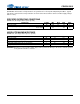
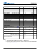
ANALOG CHARACTERISTICS (Continued)
Notes:
2. Filter response is not tested but is guaranteed by design.
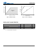
3. Response is clock dependent and will scale with Fs. Note that the response plots (Figures 15-22) have
been normalized to Fs and can be de-normalized by multiplying the X-axis scale by Fs.
4. For Base-Rate Mode, the Measurement Bandwidth is 0.5465 Fs to 3 Fs.
For High-Rate Mode, the Measurement Bandwidth is 0.577 Fs to 1.4 Fs.
5. De-emphasis is not available in High-Rate Mode.
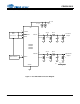
6. Refer to Figure 3.
Parameter
Base-Rate Mode High-Rate Mode
Symbol Min Typ Max Min Typ Max Unit
Combined Digital and On-chip Analog Filter Response
(Note 2)
Passband (Note 3)
to -0.05 dB corner
to -0.1 dB corner
to -3 dB corner
0
-
0
-
-
-
.4780
-
.4996
-
0
0
-
-
-
-
.4650
.4982
Fs
Fs
Fs
Frequency Response 10 Hz to 20 kHz -.01 - +.08 -.05 - +.2 dB
Passband Ripple - - ±.08 - - ±.2 dB
StopBand .5465 - - .5770 - - Fs
StopBand Attenuation (Note 4) 50 - - 55 - - dB
Group Delay tgd - 9/Fs - - 4/Fs - s
Passband Group Delay Deviation 0 - 40 kHz
0 - 20 kHz
- ±0.36/Fs - -
-
±1.39/Fs
±0.23/Fs
-
-
s
s
De-emphasis Error Fs = 32 kHz
Fs = 44.1 kHz
Fs = 48 kHz
-
-
-
-
-
-
+1.5/+0
+.05/-.25
-.2/-.4
(Note 5)
dB
dB
dB
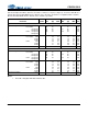
Parameters Symbol Min Typ Max Units
DC Accuracy
Interchannel Gain Mismatch - 0.1 0.4 dB
Gain Error -±5- %
Gain Drift - 100 - ppm/°C
Analog Output
Full Scale Output Voltage 3.25 3.5 3.75 Vpp
Quiescent Voltage V
Q
-2.2-VDC
Max AC-Load Resistance (Note 6) R
L
-3-k
Max Load Capacitance (Note 6) C
L
- 100 - pF