
Instruction Manual


72 DS882F1
CS42L73
The first byte sent to the CS42L73 after a Start condition consists of a 7-bit chip address field and a R/W
bit (high for a read, low for a write) in the LSB. To communicate with the CS42L73, the chip address field,
must match 1001010b.
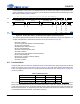
If the operation is a write, the next byte is the Memory Address Pointer (MAP); the 7 LSBs of the MAP
byte select the address of the register to be read or written to next. The MSB of the MAP byte, INCR, se-
lects whether autoincrementing is to be used (INCR = 1), allowing successive reads or writes of consec-
utive registers.
Each byte is separated by an acknowledge bit. The ACK bit is output from the CS42L73 after each input
byte is read and is input to the CS42L73 from the microcontroller after each transmitted byte.
If the operation is a write, the bytes following the MAP byte will be written to the CS42L73 register ad-
dresses pointed to by the last received MAP address, plus however many autoincrements have occurred.
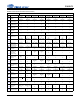
Figure 37 illustrates a write pattern with autoincrementing.
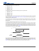
If the operation is a read, the contents of the register pointed to by the last received MAP address, plus
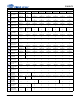
however many autoincrements have occurred, will be output in the next byte. Figure 38 illustrates a read
pattern following the write pattern in Figure 37. Notice how the read addresses are based on the MAP
byte from Figure 37.
-
4 5 6 7 24 25
SCL
CHIP ADDRESS (WRITE) MAP BYTE DATA
DATA
START
STOP
ACKACK
SDA
7 6 1 0
0 1 2 3 8 9 12 16 17 18 19 10 11 13 14 15 27 28
26
DATA
SDA
Source
Master Master Master
Pullup
Slave Slave Slave Slave
Master
Pullup
ACK ACK
7 6 5 4 3 2 1 0
MAP Addr = X
INCR = 1
Slave Addr = 1001010
7 6 5 4 3 2 1 0
R/W = 0
Data to Addr X+1
Data to Addr X+n
Master Master
Slave
Data to Addr X
7 6 1 0
7 6 1 0
Figure 37. Control Port Timing, I²C Writes with Autoincrement
SCL
DATA
STOP
ACK
ACK
SDA
7 0
7 0
CHIP ADDRESS (READ)
START
7 0
NO
258 9 184 5 6 7 0 1 2 3 16 17 34 35 36
ACK Slave Addr = 1001010
7 6 5 4 3 2 1 0
R/W = 1
DATA DATA
Data from Addr X+n+1
Data from Addr X+n+2
Data from Addr X+n+3
SDA
Source
Master
Pullup
Slave Slave Slave
Master Master Master
Pullup
27
Figure 38. Control Port Timing, I²C Reads with Autoincrement