
Instruction Manual


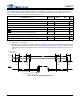

36 DS882F1
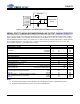
CS42L73
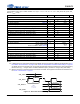
SWITCHING SPECIFICATIONS—POWER, RESET, AND MASTER CLOCKS
Test conditions (unless otherwise specified): Connections to the CS42L73 are shown in the “Typical Connection Diagram” on
page 17; GND = AGND = PGND = CPGND = DGND = 0 V; all voltages are with respect to ground (GND); VA = VCP = VL =
1.80 V, VP = 3.70 V; T
A
= +25 C; Inputs: Logic 0 = GND, Logic 1 = VL.
Notes:
52. Refer to Figure 10 on page 36.
53. Maximum frequency for highest supported nominal rate is indicated. The supported nominal MCLK1/MCLK2 rates and
their associated configurations are found in section “Internal Master Clock Generation” on page 42. Likewise, the sup-
ported nominal serial port sample rates are found in section “Serial Port Sample Rates and Master Mode Settings” on
page 53.
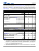
Parameters (Note 2) Symbol Min Max Units
Power Supplies (Note 52)
Power Supply Ramp Up/Down
t
pwr-rud
-
100
ms
Power Supply Ramp Skew
t
pwr-rs
-
1
s
Reset (Note 52)
RESET low (Logic 0) Pulse Width t
rlpw
1-ms
RESET Hold Time After Power Supplies Ramp Up t
rh(PWR-RH)
1-ms
RESET
Setup Time Before Power Supplies Ramp Down t
rs(RL-PWR)
1-ms
Master Clocks
MCLK1 or MCLK2 Frequency (Note 53)
-
-
38.5
MHz
MCLK1 or MCLK2 Duty Cycle
-4555
%
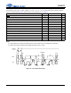
Power Supplies
(other than VP)
V
min
GND
Internal supplies stable
V
operating
t
rh(PWR-RH)
t
irs
Control port active
t
pwr-rs
t
rs(RL-PWR)
t
pwr-rs
RESET
t
pwr-rud
t
pwr-rud
t
pwr-rud
t
pwr-rud
1
st
Supply
Up
Last
Supply
Up
1
st
Supply
Down
Last
Supply
Down
Figure 10. Power and Reset Sequencing