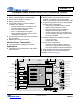
CS42L73 Ultralow Power Mobile Audio and Telephony CODEC Product Overview System Features Stereo analog-to-digital converter (ADC) Dual analog or digital mic support Dual mic bias generators Four digital-to-analog converters (DACs) coupled to five outputs – Ground-centered stereo headphone amp.
CS42L73 Stereo Analog-to-Digital Features 91-db dynamic range (A-weighted) -85 dB THD+N Independent ADC channel control 2:1 stereo analog input MUX Stereo line input: Shared pseudodifferential reference input Dual analog mic inputs – Pseudodifferential or single-ended – Two, independent, programmable, low-noise mic bias outputs – Mic short detect to support headset button Analog programmable gain amplifier (PGA) (+12 to -6 dB in 0.
CS42L73 General Description The CS42L73 is a highly integrated, low-power, audio and telephony CODEC for portable applications such as smartphones and ultramobile personal computers. The CS42L73 features a flexible clocking architecture, allowing the device to use reference clock frequencies of 6, 12, 24, 13, 26, 19.2, or 38.4 MHz, or any standard audio master clock.
CS42L73 TABLE OF CONTENTS 1. PACKAGE PIN/BALL ASSIGNMENTS AND CONFIGURATIONS ..................................................... 12 1.1 64-Ball Wafer-Level Chip Scale Package (WLCSP) ...................................................................... 12 1.2 65-Ball Fine-Pitch Ball Grid Array (FBGA) Package ...................................................................... 13 1.3 Pin/Ball Descriptions ...................................................................................................
CS42L73 4.11.2 Mixer Input Attenuation Adjustment .................................................................................... 63 4.11.3 Powered-Down Mixer Inputs ............................................................................................... 64 4.11.4 Avoiding Mixer Clipping ....................................................................................................... 64 4.11.5 Mixer Attenuation Values ........................................................................
CS42L73 6.8.4 Short Detect Automatic Mute Control .................................................................................... 86 6.9 Digital Mic and Master Clock Control (Address 0Bh) ..................................................................... 87 6.9.1 Digital Mic Shift Clock Divide Ratio ....................................................................................... 87 6.9.2 Master Clock Source Selection ............................................................................
CS42L73 6.21 Playback Digital Control (Address 19h) ..................................................................................... 100 6.21.1 Speakerphone [A], Ear Speaker/Speakerphone Line Output [B] (SES) Playback Channels B=A ............................................................................................................................ 100 6.21.2 Headphone/Line Output (HL) Playback Channels B=A .................................................... 100 6.21.3 Limiter Soft-Ramp Disable .
CS42L73 6.39.1 Limiter Maximum Threshold ESL [B] ................................................................................. 112 6.39.2 Limiter Cushion Threshold ESL [B] ................................................................................... 112 6.40 ALC Enable and Attack Rate AB (Address 2Fh) ........................................................................ 113 6.40.1 ALC for Channels A and B (ALCx) ...................................................................................
CS42L73 7.3 Layout With Fine-Pitch, Ball-Grid Packages ................................................................................ 125 8. PERFORMANCE DATA ..................................................................................................................... 126 8.1 Analog Input Path Attributes ........................................................................................................ 126 8.1.1 PGA Analog Volume Nonlinearity (DNL and INL) .....................................
CS42L73 Figure 27.I²S Format ................................................................................................................................. 55 Figure 28.PCM Format—Mode 0 .............................................................................................................. 56 Figure 29.PCM Format—Mode 1 .............................................................................................................. 56 Figure 30.PCM Format—Mode 2 ......................................
CS42L73 Table 11. Digital Mixer Soft Ramp Rates .................................................................................................. 63 Table 12. Digital Mixer Nonclipping Attenuation Settings ......................................................................... 64 Table 13. Start Up Times .......................................................................................................................... 73 Table 14. Start Up Transition Values ........................................
CS42L73 1. PACKAGE PIN/BALL ASSIGNMENTS AND CONFIGURATIONS 1.
CS42L73 1.
CS42L73 1.3 Pin/Ball Descriptions Name Location Description WLCSP FBGA MCLK1 MCLK2 A6 D6 B3 B2 High Speed Clock (Input). Potential clock sources for the converters and the device core. Clock source for optional serial port mastering. RESET E6 C9 Reset (Input). The device enters a low-power mode when this pin is driven low. SCL C3 A9 Serial Control Port Clock (Input). Serial clock for the I²C control interfaces. SDA A3 B9 Serial Control Data (Input/Output).
CS42L73 Name Location Description WLCSP FBGA LINEOUTA LINEOUTB F6 F5 G2 F2 Line Audio Output (Output). The full-scale output level is specified in the Line Output Characteristics specification table. LINEO_REF G5 H3 Pseudodifferential Line Output Reference (Input). Ground reference for the line amplifiers. EAROUT+ EAROUT- G2 H2 J8 J7 Ear Speaker Audio Output (Output). The full-scale output level is specified in the Ear Speaker Output Characteristics specification table.
CS42L73 1.
CS42L73 2. TYPICAL CONNECTION DIAGRAM VBAT PMU CS42L73 Reset Generator LDO USB +5 V RESET +1.8 V Switching +1.8 V Regulator VA VANA 0.1 µF Note 5 * VCP VDIG 2.2 µF Note 1 2.2 µF * +VCP_FILT -VCP_FILT 2.2 µF * * Other Notes: All external passive component values shown are nominal values. RP_I and RP values are defined in section “Digital Interface Specifications and Characteristics” on page 35. For the spec.
CS42L73 2.1 Low-Profile Charge-Pump Capacitors The “Typical Connection Diagram” on page 17 shows that the recommended capacitor values for the charge pump circuitry are all 2.2 F and the types are all X7R/X5R. Applications that require low-profile versions of these capacitors may use the following parts with a nominal height of only 0.5 mm: Description: 2.2 F ±20%, 6.3 V, X5R, 0402, Height = 0.5 mm Manufacturer, Part Number: • KEMET, C0402C225M9PAC 2.
CS42L73 3. CHARACTERISTIC AND SPECIFICATIONS RECOMMENDED OPERATING CONDITIONS Test Conditions: GND = AGND = PGND = CPGND = DGND = 0 V; all voltages are with respect to ground (GND).
CS42L73 ABSOLUTE MAXIMUM RATINGS Test Conditions: GND = AGND = PGND = CPGND = DGND = 0 V; all voltages are with respect to ground (GND). Parameters (Note 2) Symbol Min Max Units -0.3 -0.3 2.22 5.6 V V Iin - ±10 mA VIN-AI AGND – 0.3 VA + 0.3 VIN-AI-SD PGND – 0.3 VP + 0.
CS42L73 DC ELECTRICAL CHARACTERISTICS Test Conditions: Connections to the CS42L73 are shown in the “Typical Connection Diagram” on page 17; GND = AGND = PGND = CPGND = DGND = 0 V; all voltages are with respect to ground (GND); VA = VCP = 1.80 V, VP = 3.70 V; TA = +25 C.
CS42L73 ANALOG INPUT TO SERIAL PORT CHARACTERISTICS Test Conditions (unless otherwise specified): Connections to the CS42L73 are shown in the “Typical Connection Diagram” on page 17; Input is a 1-kHz sine wave through the passive input filter shown in Figure 1; GND = AGND = PGND = CPGND = DGND = 0 V; all voltages are with respect to ground (GND); VA = 1.
CS42L73 ANALOG INPUT TO SERIAL PORT CHARACTERISTICS (CONTINUED) Test Conditions (unless otherwise specified): Connections to the CS42L73 are shown in the “Typical Connection Diagram” on page 17; Input is a 1-kHz sine wave through the passive input filter shown in Figure 1; GND = AGND = PGND = CPGND = DGND = 0 V; all voltages are with respect to ground (GND); VA = 1.
CS42L73 MICx_BIAS -60 dBFS, 1 kHz 2.21 k 1.0 µF 100 0.1 µF 2.21 k 100 0.1 µF MICx MICx_REF Figure 2. MICx Dynamic Range Test Configuration 100 mVPP, 25 Hz 100 1 F LINEINx or MICy LINEINx_REF or MICy_REF Figure 3. Analog Input CMRR Test Setup 300 mVPP, 1 kHz LINEINx or MICx 100 0.1 µF 100 0.1 µF LINEIN_REF or MICx_REF Figure 4.
CS42L73 THERMAL OVERLOAD DETECT CHARACTERISTICS Test Conditions: Connections to the CS42L73 are shown in the “Typical Connection Diagram” on page 17; GND = AGND = PGND = CPGND = DGND = 0 V; all voltages are with respect to ground (GND); VA = 1.80 V.
CS42L73 MIC BIAS CHARACTERISTICS Test Conditions (unless otherwise specified): Connections to the CS42L73 are shown in the “Typical Connection Diagram” on page 17; GND = AGND = PGND = CPGND = DGND = 0 V; all voltages are with respect to ground (GND); VA = 1.80 V, VP = 3.70 V; TA = +25 C; IOUT = 500 A; only one bias output is powered up at a time; VP_MIN = 1b, MIC_BIAS_CTRL = 1b. Parameters (Note 2) Min Typ Max Units 1.85 2.59 2.00 2.75 2.15 2.89 V V - - 3.0 5.
CS42L73 SERIAL PORT TO STEREO HP OUTPUT CHARACTERISTICS Test conditions (unless otherwise specified): “Typical Connection Diagram” on page 17 shows CS42L73 connections (including Zobel Networks on outputs); Input test signal is a 24-bit full-scale 997-Hz sine wave with 1 LSB of triangular PDF dither applied; GND = AGND = PGND = CPGND = DGND = 0 V; all voltages are with respect to ground (GND); VA = VCP = 1.
CS42L73 SERIAL PORT TO STEREO HP OUTPUT CHARACTERISTICS (CONTINUED) Test conditions (unless otherwise specified): “Typical Connection Diagram” on page 17 shows CS42L73 connections (including Zobel Networks on outputs); Input test signal is a 24-bit full-scale 997-Hz sine wave with 1 LSB of triangular PDF dither applied; GND = AGND = PGND = CPGND = DGND = 0 V; all voltages are with respect to ground (GND); VA = VCP = 1.
CS42L73 SERIAL PORT TO STEREO LINE OUTPUT CHARACTERISTICS Test conditions (unless otherwise specified): Connections to the CS42L73 are shown in the “Typical Connection Diagram” on page 17; Input test signal is a 24-bit full-scale 997 Hz sine wave with 1 LSB of triangular PDF dither applied; GND = AGND = PGND = CPGND = DGND = 0 V; all voltages are with respect to ground (GND); VA = VCP = 1.
CS42L73 SERIAL PORT TO MONO EAR SPEAKER OUTPUT CHARACTERISTICS Test conditions (unless otherwise specified): Connections to the CS42L73 are shown in the “Typical Connection Diagram” on page 17; Input test signal is a 24-bit full-scale 997 Hz sine wave with 1 LSB of triangular PDF dither applied; GND = AGND = PGND = CPGND = DGND = 0 V; all voltages are with respect to ground (GND); VA = 1.
CS42L73 SERIAL PORT-TO-MONO SPEAKERPHONE OUTPUT CHARACTERISTICS Test conditions (unless otherwise specified): “Typical Connection Diagram” on page 17 shows CS42L73 connections; Input test signal is a 24-bit full-scale 997 Hz sine wave with 1 LSB of triangular PDF dither applied; GND = AGND = PGND = CPGND = DGND = 0 V; all voltages are with respect to ground (GND); VA = 1.80 V, VP = 3.
CS42L73 Test Load CL2 SPKOUT+ or SPKLINEO+ CL1 SPKOUTor SPKLINEO- RL + Measurement Device - CL2 PGND/AGND Figure 8.
CS42L73 STEREO/MONO DAC INTERPOLATION AND ON-CHIP DIGITAL/ANALOG FILTER CHARACTERISTICS Test Conditions (unless otherwise specified): Fs = 48 kHz (Note 10). Parameters (Note 2), (Note 47) Min Typ Max Units -0.02 - 0.10 dB - 0.48 0.50 - Fs Fs -0.29 - 0.02 dB - 0.36 0.50 - Fs Fs 0.55 - - Fs - 3.8/Fs - s Passband Ripple - 5.2x10⁻⁶ 4.4x10⁻⁵ - 0.01 Fs Fs dB Phase Deviation @ 20 Hz - 0.
CS42L73 POWER CONSUMPTION Test conditions (unless otherwise specified): Connections to the CS42L73 are shown in the “Typical Connection Diagram” on page 17; GND = AGND = PGND = CPGND = DGND = 0 V; all voltages are with respect to ground (GND); VA = VCP = VL = 1.80 V, VP = 3.70 V; TA = +25 C; RESET pin inactive; fMCLK1 = 6.144 MHz, MCLK2 is held low; Internal MCLK enabled and derived from MCLK1 input (/1) (thus, Fs = 48 kHz); fDMIC_SCLK = 1.
CS42L73 DIGITAL INTERFACE SPECIFICATIONS AND CHARACTERISTICS Test Conditions (unless otherwise specified): Connections to the CS42L73 are shown in the “Typical Connection Diagram” on page 17; GND = AGND = PGND = CPGND = DGND = 0 V; all voltages are with respect to ground (GND); VA = VL = 1.80 V, VP = 3.70 V; TA = +25 C.
CS42L73 SWITCHING SPECIFICATIONS—POWER, RESET, AND MASTER CLOCKS Test conditions (unless otherwise specified): Connections to the CS42L73 are shown in the “Typical Connection Diagram” on page 17; GND = AGND = PGND = CPGND = DGND = 0 V; all voltages are with respect to ground (GND); VA = VCP = VL = 1.80 V, VP = 3.70 V; TA = +25 C; Inputs: Logic 0 = GND, Logic 1 = VL.
CS42L73 SWITCHING SPECIFICATIONS—DIGITAL MIC INTERFACE Test conditions: Inputs: Logic 0 = GND = DGND = 0 V, Logic 1 = VL; TA = +25 C; CLOAD = 30 pF.
CS42L73 SWITCHING SPECIFICATIONS—SERIAL PORTS—I²S FORMAT Test conditions: Inputs: Logic 0 = GND = DGND = 0 V, Logic 1 = VL; TA = +25 C; x = X, A, or V; xSP_LRCK, xSP_SCLK, xSP_ SDOUT; CLOAD = 15 pF.
CS42L73 SWITCHING SPECIFICATIONS—SERIAL PORTS—PCM FORMAT Test condition: Inputs: Logic 0 = GND = DGND = 0 V, Logic 1 = VL; TA = +25 C; x = X or V; xSP_LRCK, xSP_SCLK, xSP_ SDOUT; CLOAD = 15 pF.
CS42L73 SWITCHING SPECIFICATIONS—CONTROL PORT Test conditions: Inputs: Logic 0 = GND = DGND = 0 V, Logic 1 = VL; TA = +25 C; SDA load capacitance equal to maximum value of Cb specified below (Note 58); minimum SDA pull-up resistance (RP(min)) (Note 51). Parameters (Note 2) RESET Rising Edge to Start Symbol Min (Note 52) Max Unit tirs 500 - ns SCL Clock Frequency fscl - 550 kHz Start Condition Hold Time (prior to first clock pulse) thdst 0.6 - µs Clock Low time tlow 1.
CS42L73 4. APPLICATIONS 4.1 Overview 4.1.1 Basic Architecture The CS42L73 is a highly integrated, ultralow power, 24-bit audio CODEC comprising a stereo ADC and two stereo DAC converters. The ADC is fed by pseudodifferential inputs. The DACs feed two stereo pseudodifferential output amplifiers and three mono (or one mono and one stereo, depending on configuration) full-differential amplifiers. The ADC and DAC are designed using multibit delta-sigma techniques.
CS42L73 4.2 Internal Master Clock Generation Table 1 outlines the supported internal Master Clock (MCLK) nominal frequencies and how they are derived from the supported frequencies of the external MCLK sources (MCLK1 and MCLK2). Table 1. Internal Master Clock Generation MCLK1/MCLK2 Rate (MHz) Required Divide Ratio MCLK Rate (MHz) Internal Fs (kHz) Settings for MCLKDIV[2:0] (Note 1) 5.6448 44.100 000 5.6448 1 11.2896 2 6.0000 1 12.0000 2 010 24.0000 4 100 6.1440 1 12.2880 2 13.
CS42L73 4.4 Pseudodifferential Outputs The CS42L73 provides access to the headphone and line output amplifiers’ reference inputs via the HPOUT_REF and LINEO_REF pins. These pins may be connected to either the ground at the device, or the ground return pin of each amplifier’s corresponding output connector. By routing HPOUT_REF and LINEO_REF to the ground at the device, the respective amplifier’s common mode is dictated by the ground local to the device.
CS42L73 External Impedance () 0 1 10 50 100 Maximum Attenuation Possible @ -76 dB Setting (dB) -76.0 -74.5 -72.3 -64.8 -60.0 Table 2. Example of Impedance in Reference Path 4.5 Class H Amplifier VCP ADPTPWR[2:0] Step-down/I nverting Charge Pump Class H Control +VCP +VCP/2 +VCP/3 +VCPFILT -VCP -VCP/2 -VCP/3 -VCPFILT CHGFREQ[3:0] Figure 17.
CS42L73 4.5.1.1 Standard Class AB Operation (Mode 001, 010, and 011) When the ADPTPWR is set to 001, 010, or 011, the rail voltages supplied to the amplifiers will be held to ±VCP, ±VCP/2, or ±VCP/3, respectively. For these settings, the rail voltages supplied to the output stages are held constant, regardless of the signal level, internal volume settings, or the settings of the advisory volume registers.
CS42L73 Referenced Control Register Location PDN_HP.............................. HPxAVOL ............................ HPxAMUTE ......................... PDN_LO .............................. LOxAVOL ............................ LOxAMUTE ......................... HL_PLYBCKB=A ................. HLxDMUTE ......................... HLxDVOL ............................ PDN_ADCx ......................... PDN_DMICx........................ IPB=A .................................. PGAB=A ..........................
CS42L73 +VCP Ideal Transition +VCP 2 +VCP 3 Actual Transition caused by +VCP_FILT Capacitor Time -VCP 3 -VCP 2 -VCP Figure 19. VCP_FILT Transitions When the charge pump transitions from the higher set of rail voltages to the lower set, there is a 2-second delay before the charge pump supplies the lower rail voltages to the amplifiers. This hysteresis ensures that the charge pump does not toggle between the two rail voltages as signals approach the clip threshold.
CS42L73 2 seconds 2 seconds Output Level -11 dB -15 dB Time Amplifier Rail Voltage +VCP +VCP 2 +VCP 3 Time -VCP 3 -VCP 2 -VCP Figure 20.
CS42L73 4.5.3 Efficiency As discussed in previous sections, the HPOUTx and LINEOUTx amplifiers may operate from one of three pairs of rail voltages based on the amplitude of the output signal or the relevant volume settings in the signal path. Figure 21 shows total power drawn by the device vs. power delivered to two headphone loads when the rails are held constant at each of the three available settings, or when the Class H controller is set to Adapt-to-Volume mode.
CS42L73 maximum threshold. When the input signal level falls below the maximum threshold, the AOUT volume returns to its original level set in the HP/LO Volume Control register at a programmable release rate. Attack and release rates are affected by the DAC soft ramp settings and sample rate, Fs. Limiter soft ramp dependency may be independently enabled/disabled using the LIMSRDIS. Note that the limiter maintains the output signal between the CUSHSPK, CUSHHL, CUSHESL and LMAXSPK, LMAXHL, LMAXESL thresholds.
CS42L73 4.7 Analog Output Current Limiter The CS42L73 features built-in current-limit protection for both the headphone and line output amplifiers. The approximate current through VCP during the short circuit conditions shown in Figure 23 and Figure 24 is described in Table 3. Note: 100 is always required in series with the line-output amplifiers. These amplifiers must never be shorted directly to ground.
CS42L73 • xSP_SDIN • xSP_SDOUT 4.8.3 • Toggles at external sample rate (Fsext) Serial data input Serial data output High-impedance Mode The serial ports may be placed on a clock/data bus that allows multiple masters, without the need for external buffers. The 3ST_XSP, 3ST_ASP, and 3ST_VSP bits place the internal buffers for the respective serial port interface signals in a high-impedance state, allowing another device to transmit clocks and data without bus contention.
CS42L73 The master mode supported rates for each supported MCLK are listed in the aforementioned table. The table also documents how to program the X_MMCC[5:0], A_MMCC[5:0], and V_MMCC[5:0] registers to derive the desired master mode Fsext and how much the derived Fsext rate deviates from the desired rate. 4.8.4.1 SCLK = MCLK Modes The frequency of the Serial Clock (xSP_SCLK) is programmable in master mode using the register controls X_SCLK = MCLK[1:0], A_SCLK=MCLK[1:0], and V_SCLK = MCLK[1:0].
CS42L73 Table 5. Serial Port Rates and Master Mode Settings MCLK Rate (MHz) (Note 1) 6.5000 6.4000 Standard Audio Sample Rate (kHz) Actual Master Mode xSP_ LRCK Rate (Fsext) (kHz) Deviation (%) Settings for x_ MMCC[5:0] (Note 2) 8.0000 11.0250 12.0000 16.0000 22.0500 24.0000 32.0000 44.1000 48.0000 8.0000 11.0250 12.0000 16.0000 22.0500 24.0000 32.0000 44.1000 48.0000 7.9951 11.0169 11.9926 15.9902 22.0339 23.9852 31.9803 44.0678 47.9705 8.0000 11.0345 12.0000 16.0000 22.0690 24.0000 32.0000 44.
CS42L73 4.8.6.
CS42L73 1/Fs ext 17 xSP_SCLK periods when WA is 1 xSP_SCLK period wide, 18 xSP_SCLK periods when WA is 2 xSP_SCLK periods wide xSP_LRCK (WA) xSP_SCLK may stop or continue, textra = 0 to N xSP_SCLK periods xSP_SCLK xSP_SDIN xSP_SDOUT MSB MSB MSB-1 MSB-2 MSB-3 LSB +2 LSB +1 LSB MSB MSB-1 MSB-2 MSB-3 LSB +2 LSB +1 LSB MSB MSB MSB 16 bits Note: x = X, A, or V t extra = 0, WA is 1 xSP_SCLK period wide, 1/Fsext = 17 xSP_SCLK periods textra = 1 xSP_SCLK period, WA is 1 xSP_SCLK period
CS42L73 1/Fs ext 16 xSP_SCLK periods xSP_LRCK (WA) xSP_SCLK xSP_SCLK may stop or continue xSP_SDIN MSB xSP_SDOUT MSB- 1 MSB- 2 LSB +2 LSB +1 LSB MSB textra = 0 to N xSP_SCLK periods (time between LSB and MSB data) 16 bits Note: x = X, A, or V t extra = 0, 1/Fsext = 16 xSP_SCLK periods t extra = 1 xSP_SCLK period, 1/Fsext = 17 xSP_SCLK periods textra = 2 xSP_SCLK periods, 1/Fsext = 18 xSP_SCLK periods xSP_LRCK (WA) xSP_LRCK (WA) xSP_LRCK (WA) xSP_SCLK xSP_SCLK xSP_SCLK xSP_SDIN xSP_
CS42L73 The CS42L73 will always transmit 24-bit-deep data if at least 24 serial clocks are present per channel sample. If less than 24 serial clocks are present per channel sample, it will output as many bits as there are clocks. If there are more than 24 serial clocks per channel sample, it will output zeros for the additional clock cycles after the 24th bit.
CS42L73 4.9 Asynchronous Sample Rate Converters (ASRCs) The CS42L73 uses ASRCs to bridge potentially different sample rates at the serial ports and within the Digital Processing core. Two stereo ASRCs are used for the XSP and ASP paths, one mono ASRC is used for the VSP input path, and three stereo ASRCs are used for the XSP, ASP, and VSP output paths. The Digital Processing side (as opposed to the serial port side) of the ASRCs connect to the digital mixer (refer to section “Digital Mixer” on page 41).
CS42L73 4.10.2 Digital Microphone (DMIC) Interface The DMIC Interface can be used to collect Pulse Density Modulation (PDM) audio data from the integrated ADCs of one or two digital microphones. The following sections outline how the interface may be used. 4.10.2.1 DMIC Interface Description The DMIC Interface consists of a serial-data shift clock output (DMIC_SCLK) and a serial data input (DMIC_SD).
CS42L73 4.10.2.4 DMIC Interface Clock Generation Table 10 outlines the supported DMIC Interface Serial Clock (DMIC_SCLK) nominal frequencies and how they are derived from the internal Master Clock (MCLK). Table 10. Digital Microphone Interface Clock Generation MCLK Rate (MHz) Divide Ratio DMIC_SCLK Rate (MHz) DMIC_SCLK_DIV Programming 5.6448 2 2.8224 0 4 1.4112 1 6.0000 2 3.0000 0 4 1.5000 1 6.1440 2 3.0720 0 4 1.5360 1 2 3.2500 0 4 1.6250 1 2 3.2000 0 4 1.6000 1 6.
CS42L73 Left 0 Stereo Input Path (IP) (Originating from ADCs / Digital MICs) Left 0 1 0 Right Right 2 3 Refer to section “Input Paths” on page 59 0 1 + 3 Mono Mix Right Left -6 dB Attenuation Attenuation + Stereo Headphone / Line Output (HL) Output Path Left Attenuation Right Attenuation Attenuation Attenuation + Attenuation Mono Mix -6 dB 2 Attenuation SPK_XSP_SEL[1:0] 1 -6 dB -6 dB 00 01 1x 1 + 0 1 00 01 1x 2 3 Attenuation Attenuation Attenuation + Mono Speakerphone (SP
CS42L73 4.11.1 Mono and Stereo Paths Notice how Figure 32 distinguishes between stereo and mono channels; there are buses for the stereo inputs and the digital mixer’s inputs, outputs, and programmable attenuation mixers are color coded (green for mono, blue for stereo).
CS42L73 4.11.3 Powered-Down Mixer Inputs If an input to the digital mixer is powered down (refer to register controls “Power Control 1 (Address 06h)” on page 82 and “Power Control 2 (Address 07h)” on page 83), that input must be muted. The CS42L73 does not automatically mute mixer inputs that are powered down. If a mixer input is not to be used and is not muted upstream, set the input’s attenuation to mute.
CS42L73 4.11.5 Mixer Attenuation Values The digital mixer contains fixed attenuation blocks and programmable attenuation blocks. The attenuation values associated with these blocks are as described in Figure 32 or in the related control register descriptions, except for one caveat. The caveat is the result of the binary math of the mixer circuit and design intent.
CS42L73 signal may be applied any time during the power-up sequence. If an MCLK signal is present when RESET is brought high, it is recommended that the rising edge of RESET be synchronized to the falling edge of MCLK. After RESET is brought high, the MCLK signal must not have any glitched pulses. A glitched pulse is any pulse that is shorter than the period defined by the minimum/maximum MCLK signal duty cycle specification and the nominal frequency of the MCLK; see the specifications on page 36. 4.12.
CS42L73 in “Audio ASRC Data In Lock” on page 124. 12. Start transmission of audio data to device. 13. Ramp up audio output. • Unmute the analog volume for the headphone or line amplifiers. Register Controls: HPxAMUTE/LOxAMUTE • If digital soft-ramping is used, unmute the mixer path (setting mixer volume) and/or DAC digital volume.
CS42L73 1. The CS42L73 must be put into a powered down state using the procedure in section “Power-Down Sequence (xSP to HP/LO)” on page 67. 2. The MCLK signal may then be modified or disabled at its external source (when applicable), and/or changes to the related CS42L73 control registers (see register controls list below) can be made. Use the procedure in section “Power-Up Sequence (xSP to HP/LO)” on page 66 to bring the CS42L73 out of the powered down state.
CS42L73 4.13 Using MIC2_SDET as Headphone Plug Detect Although the CS42L73 does not have a dedicated headphone plug detect pin, the MIC2_SDET pin may be used to perform a similar function. However, doing so requires that MIC2_SDET not be used as a microphone button short detect. To use the MIC2_SDET pin as a headphone detect pin, connect the headphone jack pins to the CS42L73 as shown in Figure 33. .
CS42L73 4.14 Headphone Plug Detect and Mic Short Detect To implement “headphone plug detect,” a suitable jack and system GPIO are required. Figure 35 shows two common implementations of headphone plug using additional pins within the jack. Jack detect pin type B (refer to Figure 35) is preferred, because type A requires additional filtering to remove signal from the HPOUTA pin when the headset is disconnected.
CS42L73 terrupt Status Register 2 (Address 61h)” on page 123) that are desired to cause an interrupt. The interrupt pin is either rising-edge or rising-and-falling-edge sensitive to any unmasked interrupt status change event. It will be set low when any of the unmasked status bits change state in the sensitive direction(s) and it will remain low until the status register(s) with the interrupt causing bit(s) is (are) read.
CS42L73 The first byte sent to the CS42L73 after a Start condition consists of a 7-bit chip address field and a R/W bit (high for a read, low for a write) in the LSB. To communicate with the CS42L73, the chip address field, must match 1001010b. If the operation is a write, the next byte is the Memory Address Pointer (MAP); the 7 LSBs of the MAP byte select the address of the register to be read or written to next.
CS42L73 If a read address different from that which is based on the last received MAP address is desired, an aborted write operation can be used as a preamble that sets the desired read address. This preamble technique is illustrated in Figure 39. In the figure, a write operation is aborted (after the acknowledge for the MAP byte) by sending a stop condition.
CS42L73 To use fast start mode, a set of registers must be written in a certain sequence. To enable fast start mode, perform the following sequence of register writes: 1. Register 00h = 99h 2. Register 7Eh = 81h 3. Register 7Fh = 01h 4. Register 00h = 00h To disable fast start mode, perform the following sequence of register writes: 1. Register 00h = 99h 2. Register 7Eh = 81h 3. Register 7Fh = 00h 4.
CS42L73 PDN No audio Output t=0 Clipped/Ramping audio t1 Normal audio t2 Figure 41. Start Up Transition Diagram Table 14. Start Up Transition Values Output Path 4.
CS42L73 5. REGISTER QUICK REFERENCE (Default values are shown below the bit names) I²C Address: 1001010[R/W]—10010100 = 0x94(Write); 10010101 = 0x95(Read) Adr. 00h p 81 01h p 81 02h p 81 03h p 81 04h 05h p 81 06h p 82 07h 7 6 5 4 3 2 1 0 Fast Mode Enable. FM_EN7 FM_EN6 FM_EN5 FM_EN4 FM_EN3 FM_EN2 FM_EN1 FM_EN0 0 0 0 0 0 0 0 0 Device ID A and B (Read Only). DEVIDA3 DEVIDA2 DEVIDA1 DEVIDA0 DEVIDB3 DEVIDB2 DEVIDB1 DEVIDB0 0 1 0 0 0 0 1 0 Device ID C and D (Read Only).
CS42L73 I²C Address: 1001010[R/W]—10010100 = 0x94(Write); 10010101 = 0x95(Read) Adr. 7 6 5 4 3 2 1 0 15h Mic 1 [A] PreAmp, PGAA p 98 Vol. Reserved MIC_ PREAMPA PGAAVOL5 PGAAVOL4 PGAAVOL3 PGAAVOL2 PGAAVOL1 PGAAVOL0 0 0 0 0 0 0 0 0 16h Mic 2 [B] PreAmp, PGAA p 98 Vol. Reserved MIC_ PREAMPB PGABVOL5 PGABVOL4 PGABVOL3 PGABVOL2 PGABVOL1 PGABVOL0 0 0 0 0 0 0 0 0 17h p 99 18h p 99 Input Path A Digital Volume.
CS42L73 I²C Address: 1001010[R/W]—10010100 = 0x94(Write); 10010101 = 0x95(Read) Adr. 7 6 5 4 3 2 1 0 LMAXSPK2 LMAXSPK1 LMAXSPK0 CUSHSPK2 CUSHSPK1 CUSHSPK0 Reserved Reserved 0 0 0 0 0 0 0 0 2Ch Limiter Attack Reserved Reserved 0 0 2Dh Limiter Ctl, Release Rate Ear/Speakerp 111 phone-Line [B]. LIMITESL Reserved 0 0 1 1 1 1 1 1 2Eh Limiter Thresh- Function 2Bh Limiter Thresholds Speaker- p 110 phone [A]. Rate Ear/Speakp 111 erph.-Line [B].
CS42L73 I²C Address: 1001010[R/W]—10010100 = 0x94(Write); 10010101 = 0x95(Read) Adr. 7 6 5 4 3 2 1 0 40h XSP Rt. Mixer: XSP Right p 118 Attenuation. Reserved Reserved XSPB_XSPB_ A5 XSPB_XSPB_ A4 XSPB_XSPB_ A3 XSPB_XSPB_ A2 XSPB_XSPB_ A1 XSPB_XSPB_ A0 0 0 1 1 1 1 1 1 41h XSP Left Mixer: ASP Left Attenup 118 ation. Reserved Reserved XSPA_ASPA_ A5 XSPA_ASPA_ A4 XSPA_ASPA_ A3 XSPA_ASPA_ A2 XSPA_ASPA_ A1 XSPA_ASPA_ A0 0 0 1 1 1 1 1 1 42h XSP Rt.
CS42L73 I²C Address: 1001010[R/W]—10010100 = 0x94(Write); 10010101 = 0x95(Read) Adr. Function 54h VSP Rt. Mixer: VSP Mono p 118 Attenuation. 55h Mono Mixer Controls.
CS42L73 6. REGISTER DESCRIPTION Registers are read/write except for chip ID, revision, and status registers, which are read only. The following bit definition tables show bit assignments. The default state of each bit after a power-up sequence or reset is indicated for each bit description via row shading. Reserved registers must maintain their default state. I²C Address: 1001010[R/W] 6.
CS42L73 6.4 Power Control 1 (Address 06h) 7 6 5 4 3 2 1 0 PDN_ADCB PDN_DMICB PDN_ADCA PDN_DMICA Reserved Reserved DISCHG_FILT PDN 6.4.1 Power Down ADC x Configures the power state of ADC channel x. All the analog front-end circuitry (PreAmp, PGA, etc.) associated with that channel is powered up or down according to this register bit.
CS42L73 6.5 Power Control 2 (Address 07h) 7 6 5 4 3 2 1 0 PDN_MIC2_ BIAS PDN_MIC1_ BIAS Reserved PDN_VSP PDN_ASP_ SDOUT PDN_ASP_SDIN PDN_XSP_ SDOUT PDN_XSP_SDIN 6.5.1 Power Down MICx Bias Configures the power state of the mic bias output. 6.5.2 PDN_MICx_BIAS Mic Bias Status 0 Powered Up 1 Powered Down Power Down VSP Configures the power state of the VSP. 6.5.
CS42L73 6.6 Power Control 3 and Thermal Overload Threshold Control (Address 08h) 7 6 5 4 3 2 1 0 THMOVLD_ THLD1 THMOVLD_ THLD0 PDN_THMS PDN_SPKLO PDN_EAR PDN_SPK PDN_LO PDN_HP 6.6.1 Thermal Overload Threshold Settings Configures the threshold temperature level for the Thermal Overload Interrupt Status bit. THMOVLD_THLD[1:0] Nominal Threshold Level (°C) 00 Refer to table “Thermal Overload Detect Characteristics” on page 25 01 to 11 Application: 6.6.
CS42L73 6.6.6 Power Down Line Output Configures the Output Driver power state. If the Line Output Driver or Headphone Driver is powered up, the DAC that drives them will be powered up; otherwise, it is powered down. PDN_LO 6.6.7 Line Output Driver Status 0 Powered Up 1 Powered Down Power Down Headphone Configures the Headphone Driver power state. If the Line Output Driver or Headphone Driver is powered up, the DAC that drives them will be powered up; otherwise, it is powered down. 6.
CS42L73 6.8 Output Load, Mic Bias, and MIC2 Short Detect Configuration (Address 0Ah) 7 6 5 4 3 2 1 0 Reserved VP_MIN SPK_LITE_ LOAD MIC_BIAS_ CTRL SDET_AMUTE Reserved Reserved Reserved 6.8.1 VP Supply Minimum Voltage Setting Configures the mic bias generation circuitry to accept the VP supply with the specified minimum value.
CS42L73 6.9 Digital Mic and Master Clock Control (Address 0Bh) 7 6 5 4 3 2 1 0 DMIC_SCLK_ DIV Reserved Reserved MCLKSEL MCLKDIV2 MCLKDIV1 MCLKDIV0 MCLKDIS 6.9.1 Digital Mic Shift Clock Divide Ratio Sets the divide ratio between the internal Master Clock (MCLK) and the digital mic interface shift clock output.
CS42L73 6.10 XSP Control (Address 0Ch) 7 6 3ST_XSP XSPDIF 5 4 X_PCM_MODE1 X_PCM_MODE0 3 2 1 0 X_PCM_BIT_ ORDER Reserved X_SCK=MCK1 X_SCK=MCK0 6.10.1 Tristate XSP Interface Determines the state of the XSP drivers.
CS42L73 6.11 XSP Master Mode Clocking Control (Address 0Dh) 7 6 5 4 3 2 1 0 X_M/S Reserved X_MMCC5 X_MMCC4 X_MMCC3 X_MMCC2 X_MMCC1 X_MMCC0 Refer to XSP Master Mode Clocking relevant control bits “XSP SCLK Source Equals MCLK” on page 88. 6.11.1 XSP Master/Slave Mode Applicable only if XSPDIF = 0b (I²S Format). Configures the XSP clock source (direction). Serial Port Clocks X_M/S 6.11.
CS42L73 6.12.2 ASP Sample Rate Identifies the ASP audio sample rate. ASPFS[3:0] Audio Sample Rate for ASP 0000 Don’t know 0001 8.00 kHz 0010 11.025 kHz 0011 12.000 kHz 0100 16.000 kHz 0101 22.050 kHz 0110 24.000 kHz 0111 32.000 kHz 1000 44.100 kHz 1001 48.000 kHz 1010 to 1111 Reserved Application: Refer to section “Asynchronous Sample Rate Converters (ASRCs)” on page 59. 6.12.3 ASP SCLK Source Equals MCLK Applicable only if A_M/S = 1b (Master Mode).
CS42L73 6.14 VSP Control (Address 10h) 7 6 3ST_VSP VSPDIF 5 4 V_PCM_MODE1 V_PCM_MODE0 3 2 1 0 V_PCM_BIT_ ORDER V_SDIN_LOC V_SCK=MCK1 V_SCK=MCK0 6.14.1 Tristate VSP Interface Determines the state of the VSP drivers.
CS42L73 6.14.5 VSP SDIN Location Applicable only if VSPDIF = 0b (I²S Format). Indicates if the received mono data is in the left or right portion of the frame. VSDIN_LOC Position 0 Left 1 Right Application: Refer to section “Mono/Stereo” on page 57. 6.14.6 VSP SCLK Source Equals MCLK Applicable only if VSPDIF = 0b (I²S Format) and V_M/S = 1b (Master Mode). Configures the VSP_SCLK signal source and speed. 6.
CS42L73 6.16 VSP and XSP Sample Rate (Address 12h) 7 6 5 4 3 2 1 0 VSPFS3 VSPFS2 VSPFS1 VSPFS0 XSPFS3 XSPFS2 XSPFS1 XSPFS0 6.16.1 VSP Sample Rate Identifies the VSP audio sample rate. VSPFS[3:0] Audio Sample Rate for VSP 0000 Don’t know 0001 8.00 kHz 0010 11.025 kHz 0011 12.000 kHz 0100 16.000 kHz 0101 22.050 kHz 0110 24.000 kHz 0111 32.000 kHz 1000 44.100 kHz 1001 48.
CS42L73 6.17 Miscellaneous Input and Output Path Control (Address 13h) 7 6 5 4 3 2 1 0 D_SWAP_ MONO_CTL1 D_SWAP_ MONO_CTL0 IPB=A PGAB=A PGASFT ANLGZC DIGSFT ANLGOSFT 6.17.1 Digital Swap/Mono Configures transformations on the Input Path A and B channel inputs to the digital mixer. Note that for any of the transformed cases (‘01’, ‘10’, or ‘11’), both ADC/DMIC A and B must be powered up.
CS42L73 6.17.4 PGA Soft-Ramp Configures an incremental volume ramp from the current level to the new level at the specified rate. If PGA Soft-Ramping is enabled (PGASFT = 1b), the effect of changes to the PGA analog volume controls (listed below) are applied progressively (see exceptions below); if disabled, changes are applied all at once.
CS42L73 page 96). If soft-ramping is disabled, a single volume change will occur according to the volume control change. If soft ramping is enabled, the volume change is the soft-ramp step size. With zero cross and soft-ramping enabled, with each zero cross, the volume will step until it eventually matches the volume control. 6.17.6 Digital Soft-Ramp Configures an incremental volume ramp from the present level to the new level, at the specified rate.
CS42L73 6.18 ADC/Input Path Control (Address 14h) 7 6 5 4 3 2 1 0 PGABMUX BOOSTB INV_ADCB IPBMUTE PGAAMUX BOOSTA INV_ADCA IPAMUTE 6.18.1 PGA x Input Select Selects the specified analog input signal into channel x’s PGA. PGAxMUX Selected Input to PGAA/PGAB 0 LINEINA/LINEINB 1 MIC1/MIC2 Note: For pseudodifferential inputs, the CODEC automatically chooses the respective pseudoground (LINEIN_REF or MIC1_REF, LINEIN_REF or MIC2_REF) for each input selection. 6.18.
CS42L73 6.19 Mic PreAmp and PGA Volume Control: Channel A (Mic 1, Address 15h) and Channel B (Mic 2, Address 16h) 7 6 5 4 3 2 1 0 Reserved MIC_PREAMPx PGAxVOL5 PGAxVOL4 PGAxVOL3 PGAxVOL2 PGAxVOL1 PGAxVOL0 6.19.1 Mic PREAMP x Volume Sets the gain of the mic preamp on channel x. MIC_PREAMPx Volume 0 +10 dB 1 +20 dB 6.19.2 PGAx Volume Normally, this control sets the attenuation/gain of the PGA on channel x. When the ALC is engaged, it sets the maximum volume.
CS42L73 6.20 Input Path x Digital Volume Control: Channel A (Address 17h) and B (Address 18h) 7 6 5 4 3 2 1 0 IPxDVOL7 IPxDVOL6 IPxDVOL5 IPxDVOL4 IPxDVOL3 IPxDVOL2 IPxDVOL1 IPxDVOL0 6.20.1 Input Path x Digital Volume Control Normally, this control sets the volume of the Input Path signal on channel x. When the ALC is engaged, it sets the maximum volume. Input Path digital mutes (IPxMUTE) override this register control. DS882F1 IPxDVOL[7:0] Volume 0111 1111 +12 dB ... ...
CS42L73 6.21 Playback Digital Control (Address 19h) 7 6 5 4 3 2 1 0 SES_ PLYBCKB=A HL_PLYBCKB=A LIMSRDIS Reserved ESLDMUTE SPKDMUTE HLBDMUTE HLADMUTE 6.21.1 Speakerphone [A], Ear Speaker/Speakerphone Line Output [B] (SES) Playback Channels B=A Configures independent or ganged volume control of the stereo playback channels. If ganging is enabled, channel B’s volume will be equal to channel A’s, regardless of channel B’s programming (see affected volume controls listed below).
CS42L73 6.21.5 Speakerphone Digital Mute Configures a digital mute on the volume control for speakerphone, overriding the Speakerphone digital volume setting (SPKDVOL) and the associated Limiter volume control. SPKDMUTE Speakerphone Digital Mute 0 Not muted 1 Muted 6.21.
CS42L73 6.23 Speakerphone Out [A] Digital Volume Control (Address 1Ch) 7 6 5 4 3 2 1 0 SPKDVOL7 SPKDVOL6 SPKDVOL5 SPKDVOL4 SPKDVOL3 SPKDVOL2 SPKDVOL1 SPKDVOL0 6.23.1 Speakerphone Out [A] Digital Volume Control Normally, this control sets the volume of the signal out of the Speakerphone DAC. If the Limiter is engaged, it sets the maximum volume. Speakerphone digital mutes (SPKDMUTE) override this control. 6.24 SPKDVOL[7:0] Speakerphone Volume 0001 1000 +12.
CS42L73 6.25 Headphone Analog Volume Control: Channel A (Address 1Eh) and B (Address 1Fh) 7 6 5 4 3 2 1 0 HPxAMUTE HPxAVOL6 HPxAVOL5 HPxAVOL4 HPxAVOL3 HPxAVOL2 HPxAVOL1 HPxAVOL0 6.25.1 Headphone x Analog Mute Configures an analog mute on the channel x Headphone (HP) amplifier. HPxAMUTE Headphone Amp Mute 0 Not muted 1 Muted 6.25.2 Headphone x Analog Volume Control Sets the volume of the signal out of the channel x Headphone (HP) amplifier.
CS42L73 6.26 Line Output Analog Volume Control: Channel A (Address 20h) and B (Address 21h) 7 6 5 4 3 2 1 0 LOxAMUTE LOxAVOL6 LOxAVOL5 LOxAVOL4 LOxAVOL3 LOxAVOL2 LOxAVOL1 LOxAVOL0 6.26.1 Line Output x Analog Mute Configures an analog mute on the channel x Line Output (LO) amplifier. LOxAMUTE Line Output Amp Mute 0 Not muted 1 Muted 6.26.2 Line Output x Analog Volume Control Sets the volume of the signal out of the channel x Line Output (LO) amplifier.
CS42L73 6.27 Stereo Input Path Advisory Volume (Address 22h) 7 6 5 4 3 2 1 0 STRINV7 STRINV6 STRINV5 STRINV4 STRINV3 STRINV2 STRINV1 STRINV0 Register is applicable only if ADPTPWR = 000b (Class-H power adapted to volume setting) (refer to register control description “Adaptive Power Adjustment” on page 85). 6.27.
CS42L73 6.29 ASP Input Advisory Volume (Address 24h) 7 6 5 4 3 2 1 0 ASPINV7 ASPINV6 ASPINV5 ASPINV4 ASPINV3 ASPINV2 ASPINV1 ASPINV0 Register is applicable only if ADPTPWR = 000b (Class-H power adapted to volume setting) (refer to register control description “Adaptive Power Adjustment” on page 85). 6.29.1 ASP Input Advisory Volume Defines the maximum analog input volume level used by the Class H controller to determine the appropriate supply for the Headphone and Line Output amplifiers.
CS42L73 6.31 Limiter Attack Rate Headphone/Line Output (HL) (Address 26h) 7 6 5 4 3 2 1 0 Reserved Reserved LIMARATEHL5 LIMARATEHL4 LIMARATEHL3 LIMARATEHL2 LIMARATEHL1 LIMARATEHL0 6.31.1 Limiter Attack Rate HL If limiter attack volume changes are configured to occur with a soft-ramp, this register sets the soft-ramp rate by specifying the soft-ramp step period size. 6.
CS42L73 6.33 Limiter Min/Max Thresholds Headphone/Line Output (HL) (Address 28h) 7 6 5 4 3 2 1 0 LMAXHL2 LMAXHL1 LMAXHL0 CUSHHL2 CUSHHL1 CUSHHL0 Reserved Reserved 6.33.1 Limiter Maximum Threshold HL Sets the maximum level, below full scale, above which, the Limiter will attack (increase attenuation) until the output signal’s level is below this threshold. LMAXHL[2:0] Threshold Setting 000 0 dB 001 -3 dB 010 -6 dB 011 -9 dB 100 -12 dB 101 -18 dB 110 -24 dB 111 -30 dB 6.33.
CS42L73 6.35 Limiter Control, Release Rate Speakerphone [A] (Address 2Ah) 7 6 5 4 3 2 1 0 LIMITSPK LIMIT_ALLSPK LIMRRATESPK5 LIMRRATESPK4 LIMRRATESPK3 LIMRRATESPK2 LIMRRATESPK1 LIMRRATESPK0 6.35.1 Peak Detect and Limiter Speakerphone [A] Configures the peak detect and limiter circuitry. LIMITSPK Limiter Status 0 Disabled 1 Enabled 6.35.2 Peak Signal Limit All Channels Speakerphone Sets how stereo Speakerphone channels (SPK [A] and ESL [B]) are attenuated when the limiter is enabled.
CS42L73 6.36 Limiter Min/Max Thresholds Speakerphone [A] (Address 2Bh) 7 6 5 4 3 2 1 0 LMAXSPK2 LMAXSPK1 LMAXSPK0 CUSHSPK2 CUSHSPK1 CUSHSPK0 Reserved Reserved 6.36.1 Limiter Maximum Threshold Speakerphone [A] Sets the maximum level, below full scale, above which, the Limiter will attack (increase attenuation) until the output signal’s level is below this threshold.
CS42L73 6.37 Limiter Attack Rate Ear Speaker/Speakerphone Line Output (ESL) [B] (Address 2Ch) 7 6 5 4 3 2 1 0 Reserved Reserved LIMARATEESL5 LIMARATEESL4 LIMARATEESL3 LIMARATEESL2 LIMARATEESL1 LIMARATEESL0 6.37.1 Limiter Attack Rate ESL [B] If limiter attack volume changes are configured to occur with a soft-ramp, this register sets the soft-ramp rate by specifying the soft-ramp step period size. LIMARATEESL[5:0] Step Period Size 6.
CS42L73 6.39 Limiter Min/Max Thresholds Ear Speaker/Speakerphone Line Output (ESL) [B] (Address 2Eh) 7 6 5 4 3 2 1 0 LMAXESL2 LMAXESL1 LMAXESL0 CUSHESL2 CUSHESL1 CUSHESL0 Reserved Reserved 6.39.1 Limiter Maximum Threshold ESL [B] Sets the maximum level, below full scale, above which, the Limiter will attack (increase attenuation) until the output signal’s level is below this threshold.
CS42L73 6.40 ALC Enable and Attack Rate AB (Address 2Fh) 7 6 5 4 3 2 1 0 ALCB ALCA ALCARATEAB5 ALCARATEAB4 ALCARATEAB3 ALCARATEAB2 ALCARATEAB1 ALCARATEAB0 6.40.1 ALC for Channels A and B (ALCx) Enables ALC independently for channels A and B if ALC_AB = 0b (refer to “ALC Ganging of Channels A and B” on page 116). If enabled, and if the particular channel’s signal amplitude exceeds the maximum threshold setting or falls below the minimum threshold setting, ALC is applied to only that channel.
CS42L73 6.42 ALC Threshold AB (Address 31h) 7 6 5 4 3 2 1 0 ALCMAXAB2 ALCMAXAB1 ALCMAXAB0 ALCMINAB2 ALCMINAB1 ALCMINAB0 Reserved Reserved 6.42.1 ALC Maximum Threshold for Channels A and B Sets the maximum level, below full scale, at which to limit and attenuate the input signal at the attack rate (ALCARATEAB—“ALC Attack Rate for Channels A and B” on page 113). ALCMAXAB[2:0] Threshold Setting 000 0 dB 001 -3 dB 010 -6 dB ... ... 111 -30 dB 6.42.
CS42L73 6.43 Noise Gate Control AB (Address 32h) 7 6 5 4 3 2 1 0 NGB NGA NG_BOOSTAB THRESHAB2 THRESHAB1 THRESHAB0 NGDELAYAB1 NGDELAYAB0 6.43.1 Noise Gate Enable for Channels A and B (NGx) Enables noise gating independently for channels A and B if NG_AB = 0b.
CS42L73 6.44 ALC and Noise Gate Misc Control (Address 33h) 7 6 5 4 3 2 1 0 ALC_AB NG_AB ALCBSRDIS ALCBZCDIS ALCASRDIS ALCAZCDIS Reserved Reserved 6.44.1 ALC Ganging of Channels A and B Configures whether ALC for channels A and B is independent (see “ALC for Channels A and B (ALCx)” on page 113) or ganged.
CS42L73 6.45 Mixer Control (Address 34h) 7 6 Reserved Reserved 5 4 3 VSPO_STEREO XSPO_STEREO MXR_SFTR_EN 2 1 0 MXR_STEP2 MXR_STEP1 MXR_STEP0 6.45.1 VSP Mixer Output Stereo Selects which of the following mixer outputs is sent to the VSP output: • The stereo VSP mixer outputs • The output from the mixer that combines the stereo VSP mixer’s outputs is sent to the left and right channels of the VSP output interface.
CS42L73 6.46 Stereo Mixer Input Attenuation (Addresses 35h through 54h) Sets the level of attenuation to be applied to various stereo digital mixer inputs. Each mixer input can be muted or attenuated from 0 to 62 dB in 1 dB steps. 7 6 5 4 3 2 1 0 Reserved Reserved *_A5 *_A4 *_A3 *_A2 *_A1 *_A0 Note: * indicates the field name, taken from the mixer and attenuation characteristics and listed below.. Register Addr.
CS42L73 Register Addr.
CS42L73 6.47 Mono Mixer Controls (Address 55h) 7 6 5 4 3 2 1 0 SPK_ASP_SEL1 SPK_ASP_SEL0 SPK_XSP_SEL1 SPK_XSP_SEL0 ESL_ASP_SEL1 ESL_ASP_SEL0 ESL_XSP_SEL1 ESL_XSP_SEL0 6.47.1 Speakerphone (SPK) Mixer, ASP Select Selects the input to ASP input attenuator of the SPK mono mixer. SPK_ASP_SEL[1:0] Selected Input 00 ASP Input Left Channel 01 ASP Input Right Channel 10 ASP Input Mono Mix 11 Application: Refer to section “Mono and Stereo Paths” on page 63. 6.47.
CS42L73 6.48 Mono Mixer Input Attenuation (Addresses 56h through 5Dh) Sets the level of attenuation to be applied to various mono digital mixer inputs. Each mixer input can be muted or attenuated from 0 to 62 dB in 1 dB steps. 7 6 5 4 3 2 1 0 Reserved Reserved *_A5 *_A4 *_A3 *_A2 *_A1 *_A0 Note: * indicates the field name, taken from the mixer and attenuation characteristics and listed below.. Register Addr.
CS42L73 6.49 Interrupt Mask Register 1 (Address 5Eh) The bits of this register serve as a mask for the interrupt sources found in Interrupt Status Register 1. If a mask bit is set, the interrupt is unmasked, meaning that its occurrence affects the INT pin. If a mask bit is cleared, the condition is masked, meaning that its occurrence will not affect the INT pin. The bit positions align with the corresponding bits in Interrupt Status Register 1.
CS42L73 6.51.3 Digital Mixer Overflow - Read Only; sticky; edge can trigger interrupt Indicates the over-range status in the digital mixer data path. This status bit is sticky. Rising-edge state transitions cause an interrupt, if the associated interrupt mask bit is set. DIGMIXOVFL PCM Overflow Status 0 No digital clipping has occurred in the data path of the digital mixer 1 Digital clipping has occurred in the data path of the digital mixer 6.51.
CS42L73 6.52.3 Audio ASRC Data Out Lock - Read Only; sticky; edge can trigger interrupt Indicates the lock status of the ASRC for the audio data out. This status bit is sticky. Rising-edge state transitions cause an interrupt, if the associated interrupt mask bit is set. AASRC_DOLK Status 0 Unlocked 1 Locked 6.52.4 Audio ASRC Data In Lock - Read Only; sticky; edge can trigger interrupt Indicates the lock status of the ASRC for the audio data in. This status bit is sticky.
CS42L73 6.53 Fast Mode 1 (Address 7Eh) 7 6 5 4 3 2 1 0 FM15 FM14 FM13 FM12 FM11 FM10 FM9 FM8 6.53.1 Fast Mode Bits 15:8 See “Fast Start Mode” on page 73. 6.54 Fast Mode 2 (Address 7Fh) 7 6 5 4 3 2 1 0 FM7 FM6 FM5 FM4 FM3 FM2 FM1 FM0 6.54.1 Fast Mode Bits 7:0 See “Fast Start Mode” on page 73. 7. PCB LAYOUT CONSIDERATIONS 7.
CS42L73 8. PERFORMANCE DATA Note, unless otherwise noted, the data/plots in this section are for nominal supply voltages (VA = VCP = VL = 1.80 V, VP = 3.70 V), a 25 °C ambient temperature, and were taken using the connections shown in the “Typical Connection Diagram” on page 17. 8.1 Analog Input Path Attributes 8.1.1 PGA Analog Volume Nonlinearity (DNL and INL) 0.55 12 0.54 10 0.53 8 0.52 Output Level (dB) 6 Step (dB) 0.51 0.5 0.49 4 2 0 0.48 ChA -2 0.47 0.46 ChB -4 ChA ChB 0.
CS42L73 pga_inl_mic Supply Corner, Chip 41 pga_dnl_mic Supply Corner, Chip 41 12 0.55 ChA ChB 0.54 10 0.53 8 Output Level (dB) Step (dB) 0.52 0.51 0.5 0.49 0.48 6 4 2 0 0.47 -2 0.46 -4 0.45 -6 -4 -2 0 2 4 6 PGA Setting (dB) 8 10 -6 -6 12 Figure 46. PGA + Preamp (+20 dB) DNL 8.2 ChA ChB -4 -2 0 2 4 6 PGA Setting (dB) 8 10 12 Figure 47. PGA + Preamp (+20 dB) INL Analog Mic/Line ADC and Digital Mic Input Path Attributes 8.2.1 Input Path Digital LPF Response 0 0.25 −10 0.
0 0 −10 −1 −20 −2 −30 −3 −40 −4 Magnitude (dB) Magnitude (dB) CS42L73 −50 −60 −5 −6 −70 −7 −80 −8 −90 −9 −100 0.4 0.45 0.5 0.55 0.6 Frequency (normalized to Fs) −10 0.45 0.65 Figure 50. Input Path LPF Transition Band 8.2.2 0.46 0.47 0.48 0.49 0.5 0.51 Frequency (normalized to Fs) 0.52 0.53 0.54 0.55 Figure 51. Input Path LPF Transition Band Detail Input Path Digital HPF Response 0.5 0 −0.5 Amplitude in dB −1 −1.5 −2 −2.5 −3 −3.5 0 0.2 0.4 0.6 0.8 1 1.
CS42L73 8.3 Core Circuitry Attributes 8.3.1 ASRC Attributes 8.3.1.1 Response The following curves illustrate the ASRC frequency response. The horizontal frequency axis is normalized to the external Fs (Fsext, the serial port sample rate), because for all external Fs values, the plots are exactly the same—only the scaling of the horizontal axis changes.
CS42L73 8.3.1.2 Group Delay The group-delay equations for the ASRCs are specified in “ASRC Digital Filter Characteristics” on page 25. The following chart illustrates, for the extreme supported internal sample rates (Fs) and standard audio sample rates, the input (from the serial ports to the core) and output (from the core to the serial ports) group delays through the ASRCs. ASRC Group Delay vs. Serial Port and Internal Sample Rates 1.00 Input, Fs = 44.1 kHz Input, Fs= 50.781 kHz Output, Fs = 44.
CS42L73 8.4 Analog Output Paths Attributes 8.4.1 DAC Digital LPF Response 0 0.25 −10 0.2 −20 0.15 −30 Magnitude (dB) Magnitude (dB) 0.1 0.05 0 −0.05 −40 −50 −60 −0.1 −70 −0.15 −80 −0.2 −90 −0.25 0 0.05 0.1 0.15 0.2 0.25 0.3 Frequency (Normalised to Fs) 0.35 0.4 0.45 Figure 56. DAC LPF Frequency Response 0.5 −100 0 0.1 0.2 0.3 0.4 0.5 0.6 Frequency (Normalised to Fs) 0.7 0.8 0.9 1 Figure 57.
CS42L73 8.4.2 DAC HPF Response 0.5 0 −0.5 Amplitude in dB −1 −1.5 −2 −2.5 −3 −3.5 0 0.2 0.4 0.6 0.8 1 1.2 Normalised to Fs 1.4 1.6 1.8 2 −3 x 10 Figure 59. DAC HPF Frequency Response 8.4.3 Output Analog Volume Nonlinearity (DNL and INL) _ _ p_ pp y , _ _ p_ p , p ChA ChA 1.08 pp y 2.1 1.1 ChB ChB 2.05 1.06 2 Actual Step Size (dB) Actual Step Size (dB) 1.04 1.02 1 0.98 1.95 1.9 1.85 0.96 1.8 0.94 1.75 0.92 0.
CS42L73 _ _ 1.1 p ChA ChA ChB ChB 2.05 1.05 2 Actual Step Size (dB) Actual Step Size (dB) pp y 2.1 1 0.95 1.95 1.9 1.85 1.8 1.75 0.9 -50 -40 -30 -20 -10 0 DAC Analog Volume Setting (dB) Figure 64. LINEOUTx DNL (-50 to +12 dB) _ _ 10 pp y 1.7 10 -75 -70 -65 -60 DAC Analog Volume Setting (dB) -55 Figure 65.
CS42L73 9. PARAMETER DEFINITIONS Dynamic Range The ratio of the rms value of the signal to the rms sum of all other spectral components over the specified bandwidth. Dynamic range is a signal-to-noise ratio measurement over the specified band width made with a -60 dB signal. 60 dB is added to resulting measurement to refer the measurement to full-scale. This technique ensures that the distortion components are below the noise level and do not affect the measurement.
CS42L73 10.PACKAGE DIMENSIONS 10.1 WLCSP Package 64-Ball WLCSP (3.44 x 3.44 mm Body) Package Drawing X X A2 Location Indicator (Seen Through Package) A M A1 Ball A1 Ball A1 Location Indicator Y N Z e Y WAFER BACK SIDE d b øb Øddd Z X Y Øccc Z Seating plane SIDE VIEW e c BUMP SIDE Notes: • Dimensioning and tolerances per ASME Y 14.5M–1994. • The Ball A1 position indicator is for illustration purposes only and may not be to scale.
CS42L73 10.2 FBGA Package 65-Ball FBGA (5 x 5 mm Body) Package Drawing X X A2 Ball A1 Location Indicator A M A1 Ball A1 Ball A1 Location Indicator Y N Z e b øb Øddd Z X Y Øccc Z Y Seating plane TOP SIDE d SIDE VIEW e c BUMP SIDE Notes: • Dimensioning and tolerances per ASME Y 14.5M–1994. • The Ball A1 position indicator is for illustration purposes only and may not be to scale.
CS42L73 11.THERMAL CHARACTERISTICS Parameter (Notes 1 and 2) Symbol Min Typ Max Units Junction to Ambient Thermal Impedance JA - 43 - °C/Watt Junction to Printed Circuit Board Thermal Impedance JB - 10 - °C/Watt Junction to Ambient Thermal Impedance JA - 58 - °C/Watt Junction to Printed Circuit Board Thermal Impedance JB - 12 - °C/Watt WLCSP Package FBGA Package Notes: 1. 2.
CS42L73 14.REVISION HISTORY Revision Changes F1 • Removed all references to PDN_LDO. • Updated Stereo DAC to Headphone Amplifier: High HP power output and Mono DAC to Speakerphone Amplifier: High output power on page 2. • Added (Note 4) to Absolute Maximum Ratings on page 20. Added a cross-reference to this note in Section 4.12.1 and Section 4.12.6. • Added Analog Output Current Limiter On Threshold specification to DC Electrical Characteristics on page 21.
CS42L73 Contacting Cirrus Logic Support For all product questions and inquiries, contact a Cirrus Logic Sales Representative. To find one nearest you, go to www.cirrus.com. IMPORTANT NOTICE Cirrus Logic, Inc. and its subsidiaries (“Cirrus”) believe that the information contained in this document is accurate and reliable. However, the information is subject to change without notice and is provided “AS IS” without warranty of any kind (express or implied).