
User Manual


DS851F2 57
CS42L56
6. REGISTER DESCRIPTION
All registers are read/write except for the chip I.D. and revision register and the status register which are read only.
See the following bit definition tables for bit assignment information. The default state of each bit after a power-up
sequence or reset is listed in each bit description. Unless otherwise specified, all “Reserved” bits must maintain their
default value.
6.1 Device I.D. Register (Address 01h) (Read Only)
6.1.1 Device I.D. (Read Only)
Device I.D. code for the CS42L56.
6.2 Device Revision Register (Address 02h) (Read Only)
6.2.1 Alpha Revision (Read Only)
CS42L56 alpha revision level.
6.2.2 Numeric Revision (Read Only)
CS42L56 numeric revision level.
6.3 Power Control 1 (Address 03h)
6.3.1 Power Down VCM Bias Buffer
Configures the power state of the weak internal VCM buffer.
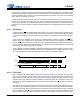
I²C Address: 1001010[R/W]
76543210
DEVID7 DEVID6 DEVID5 DEVID4 DEVID3 DEVID2 DEVID1 DEVID0
DEVID[7:0] Part Number
01010110 CS42L56
76543210
Reserved Reserved Reserved AREVID2 AREVID1 AREVID0 MTLREVID1 MTLREVID0
AREVID[2:0] Alpha Revision Level
000 A
MTLREVID[1:0] Metal Revision Level
00 0
76543210
Reserved Reserved PDN_VBUF PDN_BIAS PDN_CHRG PDN_ADCB PDN_ADCA PDN
PDN_VBUF Weak VCM Status
0
All weak VCM buffers for the AINx inputs that are not selected (either through ADCxMUX[1:0] or PGAx-
MUX[1:0]) are powered up. The weak VCM buffers for the AINx inputs that are selected are powered down.
1 All weak VCM buffers are powered down.
Application: “Optional VCM Buffer” on page 35