
User Manual


DS851F2 33
CS42L56
If signals larger than what is shown in Table 1 are needed, an external resistor divider should be used as
shown in Table 15. When using an external resistor divider, the PGA must be configured to be in-circuit.
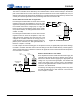
Three parameters determine the values of resistors R1 and R2 as shown in Figure 15: source impedance,
attenuation, and input impedance. Table 2 shows the design equation used to determine these values.
• Source Impedance: Source impedance is defined as the impedance as seen from the PGA looking
back into the signal network. The PGA achieves optimal THD+N performance with a source imped-
ance less than 5 k.
• Attenuation: The required attenuation factor depends on the magnitude of the input signal. The full-
scale input voltage is specified under “Analog Input Characteristics” on page 14. The user should se-
lect values for R1 and R2 such that the magnitude of the incoming signal multiplied by the attenuation
factor is less than or equal to the full-scale input voltage of the device.
• Input Impedance: Input impedance is the impedance from the signal source to the PGA analog input
pins, including the PGA. The PGA’s input impedance (R3 in Figure 15, Table 2, and Figure 16) is giv-
en in the “Analog Input Characteristics” on page 14.
Figure 16 illustrates an example configuration with the PGA in-circuit using one 7.87 kresistor for R1
and one 4.75 k resistor for R2. Based on the discussion above, this circuit provides an optimal interface
for both the PGA and the signal source. First, consumer equipment frequently requires an approximate
input impedance of 10 kwhich the combination of the resistors provide. Second, this circuit will attenu-
ate a typical line level voltage, 2 Vrms, to the full-scale input of the PGA, 0.7 Vrms when VA = 2.5 V. Fi-
nally, at approximately 3 kthe source impedance is within the allowable range of the PGA.
Source Impedance
Attenuation Factor
Input Impedance
Table 2. Analog Input Design Parameters
Figure 15. Analog Input Attenuation
AINxx
Input
R1
R2
1µF
R3
R1 R2
R1 R2+
-------------------------
R2 R3
R1 R2 R2 R3 R1 R3++
------------------------------------------------------------------------------
R1 R3 R2 R3+
R1 R2 R3++
---------------------------------------------------
AINxx
Input
Figure 16. Example Analog Input Attenuation
7.87 k
4.75 k
1µF
R3