
User Manual


32 DS851F2
CS42L56
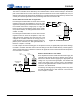
4.2.1 Pseudo-differential Inputs
The CS42L56 implements a pseudo-differential input stage. The AINxREF inputs are intended to be used
as a pseudo-differential reference signal. This feature provides common mode noise rejection with single-
ended signals. Figure 14 shows a basic diagram outlining the internal implementation of the pseudo-dif-
ferential input stage, including a recommended stereo pseudo-differential input topology. If pseudo-differ-
ential input functionality is not required, the AINxREF pin should be AC-coupled to GND.
It should be noted that the AINxREF inputs are intended to be used solely to provide a low-level, pseudo-
differential reference signal for the internal input amplifiers when in pseudo-differential mode. Using the
analog input pins in a fully differential configuration by providing a large signal on the AINxREF pin is not
recommended. The output of the PGA will clip if the voltage difference between AINxx and AINxREF ex-
ceeds the full-scale voltage specification (See Note 10 on page 17).
4.2.2 Large-scale Inputs
The CS42L56 allows the user to input signals that would be larger than the ADC full-scale input voltage
by using the PGA to attenuate the signal prior to going to the ADC. Table 1 shows the PGA gain setting
needed to stay under the maximum ADC input voltage.
Supply Voltage PGA Gain Setting Maximum Input Voltage
(V) (dB)
(mV
RMS
)(V
PP
)
1.8
0.0 509 1.44
-0.5 539 1.52
-1.0 571 1.62
-1.5 604 1.71
2.5
0.0 707 2.00
-0.5 748 2.12
-1.0 793 2.24
-1.5 840 2.38
Table 1. Input Voltage PGA Settings
xIN
xREF
Signal+
Anti-
Aliasing
Filter
Common-Mode Cancellation,
Invert, and Gain
AFILTx
DC-Block
VA
VQ
AGND
VCM
R
R
ADC
Parallel PCB
traces from
signal source
Digital
Full Scale
VCM
VCM
V=?
VCM
VCM
-
+
-
+
Figure 14. Stereo Pseudo-Differential Input