
User Manual


14 DS851F2
CS42L56
3. CHARACTERISTIC AND SPECIFICATION TABLES
RECOMMENDED OPERATING CONDITIONS
GND = AGND = 0 V; all voltages with respect to ground.
ABSOLUTE MAXIMUM RATINGS
GND = AGND = 0 V; all voltages with respect to ground.
WARNING: Operation at or beyond these limits may result in permanent damage to the device. Normal operation
is not guaranteed at these extremes.
Notes:
1. Due to the existence of parasitic body diodes between VCP and VA, current flows from VCP to VA when-
ever the VA power supply is lower than VCP. This causes a “back-powering” effect on the VA power
supply rails internal to the part; therefore, VA should be maintained at an equal or greater voltage than
VCP at all times. While “back-powering” does not have any adverse effects on device operation with
respect to performance and reliability, it does lead to extra power consumption and therefore should be
avoided.
2. Any pin except supplies. Transient currents of up to ±100 mA on the analog input pins will not cause
SCR latch-up.
3. The maximum over/under voltage is limited by the input current.
4. VHPFILT is specified in “DC Characteristics” on page 27.
Parameters Symbol Min Max Units
DC Power Supply
Analog (Note 1) VA 1.62 2.75 V
Charge Pump (Note 1) VCP 1.62 VA V
LDO Regulator for Digital VLDO 1.62 2.75 V
Serial/Control Port Interface VL 1.62 3.63 V
Ambient Temperature Commercial - CNZ T
A
-40 +85 C
Parameters Symbol Min Max Units
DC Power Supply Analog, Charge Pump, LDO
Serial/Control Port Interface
VA, VCP, VLDO
VL
-0.3
-0.3
3.0
4.0
V
V
Input Current (Note 2) I
in
-±10mA
External Voltage Applied to Analog Input (Note 3)
V
IN
AGND-0.3 VA+0.3
V
External Voltage Applied to Analog Output (Note 4)
V
IN
-VHPFILT - 0.3 +VHPFILT + 0.3
V
External Voltage Applied to Digital Input (Note 3) V
IND
-0.3 VL+ 0.3 V
Ambient Operating Temperature (power applied) T
A
-50 +115 °C
Storage Temperature T
stg
-65 +150 °C
ANALOG INPUT CHARACTERISTICS
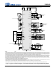
Test Conditions (unless otherwise specified): Connections to the CS42L56 are shown in the “Typical Connection Diagrams” on
page 11; Input test signal is a 1 kHz sine wave through the passive input filter, PGA = 0 dB; All Supplies = VA;
GND = AGND = 0 V; T
A
=+25C; Measurement bandwidth is 20 Hz to 20 kHz; Sample Frequency = 48 kHz. Measurement sig-
nal path is AINxx to SDOUT.
VA = 2.5 V VA = 1.8 V
Parameter
Min Typ Max Min Typ Max Unit
Analog In to ADC (PGA bypassed)