
Instruction Manual

DS773F1 9
CS42L55
1.1 I/O Pin Characteristics
Input and output levels and associated power supply voltage are shown in the table below. Logic levels
should not exceed the corresponding power supply voltage.
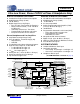
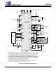
VA 17 Analog Power (Input) - Power supply for the internal analog section.
AGND 18 Analog Ground (Input) - Ground reference for the internal analog section.
FILT+ 19 Positive Voltage Reference (Output) - Positive reference voltage for the internal sampling circuits.
VQ 20 Quiescent Voltage (Output) - Filter connection for the internal quiescent voltage.
AFILTA
AFILTB
21
22
Antialias Filter Connection (Output) - Antialias filter connection for the ADC inputs.
AIN2A
AIN2B
AIN1A
AIN1B
23
25
26
28
Analog Input (Input) - The full-scale level is specified in the Analog Input Characteristics specification
table.
AIN2REF
AIN1REF
24
27
Pseudo Diff. Analog Input Reference (Input) - Ground reference for the programmable gain amplifi-
ers (PGA).
HPDETECT 29
Headphone Detect (Input) - Powers down the left and/or right channel of the line and/or headphone
outputs as described in “Headphone Power Control” on page 43 and “Line Power Control” on page 43.
RESET
30 Reset (Input) - The device enters a low power mode when this pin is driven low.
VLDO 31 Low Dropout Regulator (LDO) Power (Input) - Power supply for the LDO regulator.
VDFILT 32
Low Dropout Regulator (LDO) Filter Connection (Output) - Power supply from the LDO regulator
that provides the low voltage power to the digital section.
VL 33
Digital Interface Power (Input) - Determines the required signal level for the serial audio interface
and I²C control port.
SDOUT 34 Serial Audio Data Output (Output) - Output for two’s complement serial audio data.
MCLK 35 Master Clock (Input) - Clock source for the delta-sigma modulators.
SCLK 36 Serial Clock (Input/Output) - Serial clock for the serial audio interface.
GND/
Thermal Pad
-
Ground reference for the internal charge pump and digital section; thermal relief pad. See “QFN Ther-
mal Pad” on page 68 for more information.
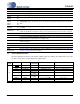
Power
Supply
Pin Name I/O Internal
Connections
Driver Receiver
VL
RESET
Input - - 1.8 V - 3.3 V, with Hysteresis
SCL Input - - 1.8 V - 3.3 V, with Hysteresis
SDA Input/Output - CMOS/Open Drain 1.8 V - 3.3 V, with Hysteresis
MCLK Input - - 1.8 V - 3.3 V
LRCK Input/Output
Weak Pull-up
(~1 MΩ)
1.8 V - 3.3 V, CMOS 1.8 V - 3.3 V
SCLK Input/Output
Weak Pull-up
(~1 MΩ)
1.8 V - 3.3 V, CMOS 1.8 V - 3.3 V
SDOUT Output - 1.8 V - 3.3 V, CMOS 1.8 V - 3.3 V
SDIN Input - - 1.8 V - 3.3 V
VA HPDETECT Input - - 1.8 V - 2.5 V, with Hysteresis