
Instruction Manual

8 DS773F1
CS42L55
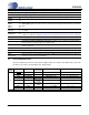
1. PIN DESCRIPTIONS
Pin Name # Pin Description
SDIN 1 Serial Audio Data Input (Input) - Input for two’s complement serial audio data.
LRCK 2
Left Right Clock (Input/Output) - Determines which channel, Left or Right, is currently active on the
serial audio data lines.
SDA 3 Serial Control Data (Input/Output) - Serial data for the I²C serial control port.
SCL 4 Serial Control Port Clock (Input) - Serial clock for the I²C serial control port.
VCP 5 Step-Down Charge Pump Power (Input) - Power supply for the step-down charge pump.
FLYP 6
Charge Pump Cap Positive Node (Output) - Positive node for the step-down charge pump’s flying
capacitor.
+VHPFILT 7
Step-Down Charge Pump Filter Connection (Output) - Power supply from the step-down charge
pump that provides the positive rail for the headphone and line amplifiers
FLYC 8
Charge Pump Cap Common Node (Output) - Common positive node for the step-down and inverting
charge pumps’ flying capacitors.
FLYN 9
Charge Pump Cap Negative Node (Output) - Negative node for the inverting charge pump’s flying
capacitor.
-VHPFILT 10
Inverting Charge Pump Filter Connection (Output) - Power supply from the inverting charge pump
that provides the negative rail for the headphone and line amplifiers.
HPOUTA
HPOUTB
11
13
Headphone Audio Output (Output) - The full-scale output level is specified in the HP Output Charac-
teristics specification table
HPREF 12 Pseudo Diff. Headphone Output Reference (Input) - Ground reference for the headphone amplifiers
LINEOUTA
LINEOUTB
14
16
Line Audio Output (Output) - The full-scale output level is specified in the Line Output Characteristics
specification table
LINEREF 15 Pseudo Diff. Line Output Reference (Input) - Ground reference for the line amplifiers.
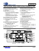
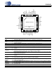
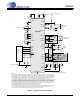
8
7
6
3
1
9
2
4
5
10 11 12 13 14 15 181716
19
26
20
21
22
23
24
25
27
35 28
293031
32
333436
VLDO
VDFILT
VL
MCLK
SDOUT
HPOUTA
HPREF
HPOUTB
LINEOUTA
LINEREF
VA
LINEOUTB
LRCK
SDA
SCL
FLYP
HPDETECT
RESET
+VHPFILT
AIN2A
AIN2B
AFILTA
AFILTB
FILT+
VQ
AIN2REF
VCP
SDIN
AGND
SCLK
FLYN
AIN1A
AIN1REF
AIN1B
FLYC
Top-Down (Through Package)
View
-VHPFILT
GND/Thermal Pad