
Instruction Manual

42 DS773F1
CS42L55
6. REGISTER DESCRIPTION
Except for the chip I.D., revision register, and status register, which are Read Only, all registers are Read/Write. See
the following bit definition tables for bit assignment information. The default state of each bit after a power-up se-
quence or reset is listed in each bit description. All Reserved registers must maintain their default state.
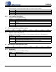
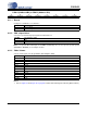
6.1 Fab I.D. and Revision Register (Address 01h) (Read Only)
6.1.1 Chip Revision (Read Only)
CS42L55 revision level.
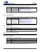
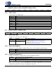
6.2 Power Control 1 (Address 02h)
6.2.1 Power Down ADC Charge Pump
Configures the power state of the ADC charge pump. For optimal ADC performance and power consump-
tion, set to ‘1’b when VA > 2.1 V and set to ‘0’b when VA < 2.1 V.
6.2.2 Power Down ADC x
Configures the power state of ADC channel x.
6.2.3 Power Down
Configures the power state of the entire CODEC.
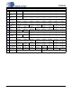
I²C Address: 1001010[R/W]
76543210
Reserved Reserved Reserved Reserved Reserved REVID2 REVID1 REVID0
REVID[2:0] Revision Level
000 A0
001 A1
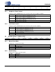
76543210
Reserved Reserved Reserved Reserved PDN_CHRG PDN_ADCB PDN_ADCA PDN
PDN_CHRG ADC Charge Pump Status
0 Powered Up
1 Powered Down
PDN_ADCx ADC Status
0 Powered Up
1 Powered Down
PDN CODEC Status
0 Powered Up
1 Powered Down