
Instruction Manual


34 DS773F1
CS42L55
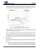
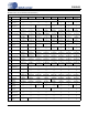
4.8 Serial Port Clocking
The CODEC serial audio interface port operates either as a slave or master. It accepts externally generated
clocks in Slave Mode (M/S
= ‘0’b) and will generate synchronous clocks derived from an input master clock
(MCLK) in Master Mode (M/S
= ‘1’b). Refer to the table below for the required setting in register 05h asso-
ciated with a given MCLK and sample rate.
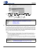
4.9 Digital Interface Format
The serial port operates in the I²S digital interface formats with varying bit depths up to 24 into the DAC and
a fixed depth of 24 out the ADC. Data is clocked out of the ADC on an internally delayed version of the rising
SCLK edge. This provides more setup time for capturing data on the rising edge of SCLK. Data is clocked
into the DAC on the rising edge of SCLK.
4.10 Initialization
The CODEC enters a Power-Down state upon initial power-up. The interpolation and decimation filters, del-
ta-sigma modulators and control port registers are reset. The charge pump, LDO, internal voltage reference
and switched-capacitor low-pass filters are powered down. The device will remain in the Power-Down state
until the RESET
pin is brought high. The control port is accessible once RESET is high and the desired reg-
ister settings can be loaded per the interface descriptions in the “Register Description” on page 42.
Referenced Control Register Location
Register 05h ........................
M/S
......................................
“Clocking Control 2 (Address 05h)” on page 44
“Master/Slave Mode” on page 43
MCLK (MHz) LRCK (kHz) Clock Ratio SPEED[1:0] 32kGROUP RATIO[1:0] Register 05h
12.0000
(MCLKDIV2=’1’b)
8.0000 1500 11 1 01 0x1D
11.0294 1088 11 0 11 0x1B
12.0000 1000 11 0 01 0x19
16.0000 750 10 1 01 0x15
22.0588 544 10 0 11 0x13
24.0000 500 10 0 01 0x11
32.0000 375 01 1 01 0x0D
44.1180 272 01 0 11 0x0B
48.0000 250 01 0 01 0x09
6.0000
(MCLKDIV2=’0’b)
8.0000 750 11 1 01 0x1D
11.0294 544 11 0 11 0x1B
12.0000 500 11 0 01 0x19
16.0000 375 10 1 01 0x15
22.0588 272 10 0 11 0x13
24.0000 250 10 0 01 0x11
32.0000 187.5 01 1 01 0x0D
44.1180 136 01 0 11 0x0B
48.0000 125 01 0 01 0x09
LRCK
SCLK
MSB LSB LSB
AOUTA / AINxA
Left Channel Right Channel
SDOUT
SDIN
AOUTB / AINxB
MSB MSB
Figure 20. I²S Format