
Instruction Manual

DS773F1 19
CS42L55
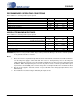
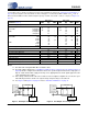
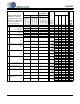
POWER SUPPLY REJECTION (PSRR) CHARACTERISTICS
Test Conditions (unless otherwise specified): Connections to the CS42L55 are shown in the “Typical Connection Diagram” on
page 10; GND = AGND = 0 V; all voltages with respect to ground.
Notes:
20. Valid with the recommended capacitor values on FILT+ and VQ, no load on HP and Line. Increasing
the capacitance on FILT+ and VQ will also increase the PSRR.
21. The PGA is biased with VQ, created by a resistor divider from the VA supply.
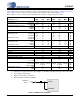
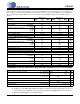
DIGITAL INTERFACE SPECIFICATIONS & CHARACTERISTICS
22. See “I/O Pin Characteristics” on page 9 for serial and control port power rails.
Parameters Min Typ Max Units
PSRR with 100 mVpp, 1 kHz signal (Note 20) PGA to ADC
ADC
PGA to HP & Line Amps
DAC to HP & Line Amps
-
-
-
-
55
50
50
50
-
-
-
-
dB
dB
dB
dB
PSRR with 100 mVpp, 60 Hz signal (Note 20) PGA to ADC (Note 21)
ADC
PGA to HP & Line Amps
DAC to HP & Line Amps
-
-
-
-
35
25
50
60
-
-
-
-
dB
dB
dB
dB
Parameters (Note 22) Symbol Min Max Units
Input Leakage Current
I
in
-±10μA
Input Capacitance
-10pF
1.8 V - 3.3 V Logic
High-Level Output Voltage (I
OH
= -100 μA)
V
OH
VL - 0.2 - V
Low-Level Output Voltage (I
OL
= 100 μA)
V
OL
-0.2V
High-Level Input Voltage VL = 1.65 V
VL = 1.8 V
VL = 2.0 V
VL > 2.0 V
V
IH
0.83•VL
0.76•VL
0.68•VL
0.65•VL
-
-
-
-
V
Low-Level Input Voltage
V
IL
-0.30•VLV
HPDETECT Input
High-Level Input Voltage
HPDV
IH
0.65•VA - V
Low-Level Input Voltage
HPDV
IL
-0.35•VAV
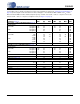
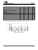
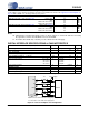
VCP
GND/AGND
Voltmeter
-
+
1 Ω
Power Supply
-
+
1 Ω
-
+
1 Ω
-
+
1 Ω
VA
VLDO
VL
2.2 µF
0.1 µF
0.1 µF
0.1 µF
Note: Current is derived from the voltage drop across
a 1 Ω resistor in series with each supply input.
Figure 8. Power Consumption Test Configuration