
Instruction Manual

DS773F1 17
CS42L55
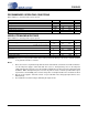
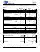
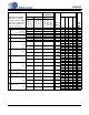
SWITCHING SPECIFICATIONS - SERIAL PORT
Inputs: Logic 0 = GND = AGND, Logic 1 = VL, LRCK, SCLK, SDOUT C
LOAD
= 15 pF.
Notes: 17. After powering up the CS42L55, RESET should be held low after the power supplies and clocks are
settled. This specification is valid with the recommended capacitor on VDFILT.
18. The device will periodically extend the SCLK high time to compensate for the fractional MCLK/SCLK
ratio.
Parameters Symbol Min Max Units
RESET pin Low Pulse Width (Note 17)
1
-ms
MCLK Frequency
(See “Serial Port Clocking”
on page 34)
MHz
MCLK Duty Cycle 45 55 %
Slave Mode (Figure 5)
Input Sample Rate (LRCK) F
s
(See “Serial Port Clocking”
on page 34)
kHz
LRCK Duty Cycle 45 55 %
SCLK Frequency 1/t
Ps
- 68•F
s
Hz
SCLK Duty Cycle 45 55 %
LRCK Setup Time Before SCLK Rising Edge t
ss(LK-SK)
40 - ns
SDOUT Setup Time Before SCLK Rising Edge t
ss(SDO-SK)
20 - ns
SDOUT Hold Time After SCLK Rising Edge t
hs(SK-SDO)
30 - ns
SDIN Setup Time Before SCLK Rising Edge t
ss(SD-SK)
20 - ns
SDIN Hold Time After SCLK Rising Edge t
hs
20 - ns
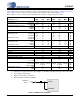
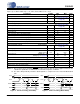
Master Mode (Figure 6)
Output Sample Rate (LRCK) All Speed Modes
F
s
(See “Serial Port Clocking”
on page 34)
Hz
LRCK Duty Cycle 45 55 %
SCLK Frequency SCLK = MCLK mode 1/t
Pm
- 12.0000 MHz
All Other Modes 1/t
Pm
- 68•F
s
Hz
SCLK Duty Cycle RATIO[1:0] = ‘11’ 45 55 %
RATIO[1:0] = ‘01’ (Note 18) 33 66 %
LRCK Time Before SCLK Falling Edge t
sm(LK-SK)
-±2ns
SDOUT Setup Time Before SCLK Rising Edge t
sm(SDO-SK)
20 - ns
SDOUT Hold Time After SCLK Rising Edge t
hm(SK-SDO)
30 - ns
SDIN Setup Time Before SCLK Rising Edge t
sm(SD-SK)
20 - ns
SDIN Hold Time After SCLK Rising Edge t
hm
20 - ns
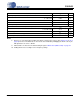
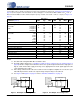
t
hs(SK-SDO)
//
//
//
//
//
//
//
//
t
ss(SD-SK)
MSB
MSB
LRCK
SCLK
SDOUT
SDIN
t
ss(LK-SK)
t
P
t
hs
t
ss(SDO-SK)
//
//
//
//
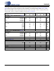
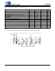
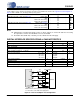
Figure 5. Serial Port Timing (Slave Mode) Figure 6. Serial Port Timing (Master Mode)
t
hm(SK-SDO)
//
//
//
//
//
//
//
//
t
sm(SD-SK)
MSB
MSB
LRCK
SCLK
SDOUT
SDIN
t
Pm
t
hm
t
sm(SDO-SK)
//
//
//
//
//
//
t
sm(LK-SK)