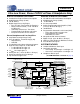
CS42L55 Ultra Low Power, Stereo CODEC w/Class H Headphone Amp DIGITAL to ANALOG FEATURES ANALOG to DIGITAL FEATURES 5 mW Stereo Playback Power Consumption 99 dB Dynamic Range (A-wtd) -86 dB THD+N Digital Signal Processing Engine – Bass & Treble Tone Control, De-Emphasis – Master Volume Control (+12 to -102 dB in 0.
CS42L55 SYSTEM FEATURES High Performance 24-bit Converters – Multi-bit Delta Sigma Architecture Integrated High Efficient Power Management Reduces Power Consumption – Step-Down Charge Pump Improves Efficiency – Inverting Charge Pump Accommodates Low System Voltage by Providing Negative Rail for HP/Line Amp – LDO Reg.
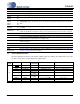
CS42L55 TABLE OF CONTENTS 1. PIN DESCRIPTIONS .............................................................................................................................. 8 1.1 I/O Pin Characteristics ...................................................................................................................... 9 2. TYPICAL CONNECTION DIAGRAM ................................................................................................... 10 3. CHARACTERISTIC AND SPECIFICATION TABLES ............
CS42L55 5. REGISTER QUICK REFERENCE ........................................................................................................ 40 6. REGISTER DESCRIPTION .................................................................................................................. 42 6.1 Fab I.D. and Revision Register (Address 01h) (Read Only) ........................................................... 42 6.1.1 Chip Revision (Read Only) ......................................................................
CS42L55 6.13.4 Invert PCM Signal Polarity .................................................................................................. 51 6.13.5 Master Playback Mute ......................................................................................................... 51 6.14 ADCx Mixer Volume: ADCA (Address 10h) & ADCB (Address 11h) ...................................................................................... 51 6.14.1 ADC Mixer Channel x Mute .............................................
CS42L55 6.30 ALC Release Rate (Address 25h) ................................................................................................ 63 6.30.1 ALC Release Rate ............................................................................................................... 63 6.31 ALC Threshold (Address 26h) ...................................................................................................... 64 6.31.1 ALC Maximum Threshold .............................................................
CS42L55 Figure 18.Beep Configuration Options ...................................................................................................... 32 Figure 19.Peak Detect & Limiter ............................................................................................................... 33 Figure 20.I²S Format ................................................................................................................................. 34 Figure 21.Control Port Timing, I²C Write ...................
CS42L55 Pin Name # SCLK MCLK SDOUT VL VDFILT VLDO RESET HPDETECT AIN1B 1.
CS42L55 VA 17 Analog Power (Input) - Power supply for the internal analog section. AGND 18 Analog Ground (Input) - Ground reference for the internal analog section. FILT+ 19 Positive Voltage Reference (Output) - Positive reference voltage for the internal sampling circuits. VQ 20 Quiescent Voltage (Output) - Filter connection for the internal quiescent voltage. AFILTA AFILTB 21 22 Antialias Filter Connection (Output) - Antialias filter connection for the ADC inputs.
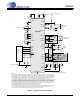
CS42L55 2. TYPICAL CONNECTION DIAGRAM 1 µF ** ** VDFILT 0.1 µF VLDO ** +1.65 V to +2.71 V 0.1 µF VA 47 kΩ +VHPFILT HPREF ** 2.2 µF 0.1 µF HPOUTB Note 1 +1.65 V to +2.71 V 33 Ω HPOUTA VCP 2.2 µF ** Headphone Out Left & Right 33 Ω ** 0.1 µF ** HPDETECT CS42L55 Note 2 2.2 µF ** 2.2 µF ** FLYP FLYC LINEOUTA 562 Ω 3300 pF FLYN LINEOUTB Note 1 2.
CS42L55 3. CHARACTERISTIC AND SPECIFICATION TABLES RECOMMENDED OPERATING CONDITIONS GND = AGND = 0 V, all voltages with respect to ground. Parameters DC Power Supply Analog Charge Pump LDO Regulator for Digital Serial/Control Port Interface Ambient Temperature Commercial - CNZ Symbol Min Max Units VA VCP VLDO VL TA 1.65 1.65 1.65 1.65 -40 2.71 VA 2.71 3.47 +85 V V V V °C Symbol Min Max Units 3.0 4.0 ±10 VA+0.7 VL+0.
CS42L55 ANALOG INPUT CHARACTERISTICS Test Conditions (unless otherwise specified): Connections to the CS42L55 are shown in the Figure 1. "Typical Connection Diagram" on page 10; Input is a 1 kHz sine wave through the passive input filter, PGA = 0 dB; All Supplies = VA; GND = AGND = 0 V; TA = +25°C; Measurement bandwidth is 20 Hz to 20 kHz. Sample Frequency = 48 kHz. VA = 2.
CS42L55 ADC DIGITAL FILTER CHARACTERISTICS Parameter (Note 8) Frequency Response (20 Hz to 20 kHz) Passband to -0.05 dB corner to -3 dB corner Stopband Stopband Attenuation Total Group Delay Min Typ Max Unit -0.07 - +0.02 dB - 0.421 0.495 - Fs Fs 0.52 - - Fs 33 - - dB - 7.6/Fs - s - 1.87 17.15 - Hz Hz High-Pass Filter Characteristics (48 kHz Fs) (Note 9) Passband to -3.0 dB corner to -0.05 dB corner Passband Ripple - - 0.15 dB Phase Deviation - 5.
CS42L55 HP OUTPUT CHARACTERISTICS Test conditions (unless otherwise specified): Connections to the CS42L55 are shown in the “Typical Connection Diagram” on page 10; Input test signal is a full-scale 997 Hz sine wave; All Supplies = VA, VCP Mode; GND = AGND = 0 V; TA = +25°C; Measurement bandwidth is 20 Hz to 20 kHz; Sample Frequency = 48 kHz; Test load RL = 3 kΩ, CL = 150 pF for a Line Load, and test load RL = 16 Ω, CL = 150 pF for a headphone load. (See Figure 3 on page 15). VA = 2.
CS42L55 LINE OUTPUT CHARACTERISTICS Test conditions (unless otherwise specified): Connections to the CS42L55 are shown in the “Typical Connection Diagram” on page 10; Input test signal is a full-scale 997 Hz sine wave; All Supplies = VA, VCP Mode; GND = AGND = 0 V; TA = +25 °C; Measurement bandwidth is 20 Hz to 20 kHz; Sample Frequency = 48 kHz; Test load RL = 3 kΩ, CL = 150 pF (see Figure 3 on page 15). VA = 2.
CS42L55 ANALOG PASSTHROUGH CHARACTERISTICS Test Conditions (unless otherwise specified): Connections to the CS42L55 are shown in the “Typical Connection Diagram” on page 10; Input is a 1 kHz sine wave through the passive input filter shown in Figure 1, PGA and HP/Line gain = 0 dB; All Supplies = VA, VCP Mode; GND = AGND = 0 V; TA = +25 °C; Measurement bandwidth is 20 Hz to 20 kHz. Sample Frequency = 48 kHz. Parameter Min VA = 2.5 V Typ Max Min VA = 1.
CS42L55 SWITCHING SPECIFICATIONS - SERIAL PORT Inputs: Logic 0 = GND = AGND, Logic 1 = VL, LRCK, SCLK, SDOUT CLOAD = 15 pF.
CS42L55 SWITCHING SPECIFICATIONS - CONTROL PORT Inputs: Logic 0 = GND = AGND, Logic 1 = VL, SDA CL = 30 pF. Parameter Symbol Min Max Unit fscl - 100 kHz RESET Rising Edge to Start tirs 500 - ns Bus Free Time Between Transmissions tbuf 4.7 - µs Start Condition Hold Time (prior to first clock pulse) thdst 4.0 - µs Clock Low time tlow 4.7 - µs Clock High Time thigh 4.0 - µs Setup Time for Repeated Start Condition tsust 4.
CS42L55 POWER SUPPLY REJECTION (PSRR) CHARACTERISTICS Test Conditions (unless otherwise specified): Connections to the CS42L55 are shown in the “Typical Connection Diagram” on page 10; GND = AGND = 0 V; all voltages with respect to ground.
CS42L55 POWER CONSUMPTION - ALL SUPPLIES = 1.8 V ADCAMUX[1:0] ADCBMUX[1:0] PDN_LINA[1:0] PDN_LINB[1:0] PDN_HPA[1:0] x x x x x x x x x x 0.001 0.01 x x x x x x x x x x - 0.003 0.002 0.039 0.006 0.09 MCLKDIS=0 x x x 1 x x x x x x x x x x x - 0.002 0.005 0.223 0.006 0.43 (Note 23) MCLKDIS=x x x x 1 x x x x x x x x x x x - 0.002 0.002 0.010 0.002 0.03 ADC 0 1 0 0 11 11 11 11 xx 01 x x x x x - 0.003 0.859 0.650 0.017 2.
CS42L55 POWER CONSUMPTION - ALL SUPPLIES = 2.5 V PDN_ADCB PDN_ADCA PDN ADCAMUX[1:0] LINEBMUX LINEAMUX HPBMUX HPAMUX PDN_DSP - 0Fh page 50 x x x x x x x x x x x x x x x x x 1 x x x x x x x x x x x - 0.000 0.000 0.064 0.007 0.18 MCLKDIS=0 x x x 1 x x x x x x x x x x x - 0.000 0.013 0.385 0.007 1.01 (Note 23) MCLKDIS=x x x x 1 x x x x x x x x x x x - 0.000 0.000 0.018 0.000 0.05 ADC 1 1 0 0 11 11 11 11 xx 01 x x x x x - 0.000 0.752 0.743 0.019 3.
CS42L55 4. APPLICATIONS 4.1 4.1.1 Overview Basic Architecture The CS42L55 is a highly integrated, ultra-low power, 24-bit audio CODEC comprised of stereo A/D and D/A converters with pseudo-differential stereo input and output amplifiers. The ADC and DAC are designed using multi-bit delta-sigma techniques; both converters operate at a low oversampling ratio of 64xFs, maximizing power savings while maintaining high performance.
CS42L55 4.
CS42L55 4.2.1 Pseudo-Differential Inputs The CS42L55 implements a pseudo-differential input stage. The AINxREF inputs are intended to be used as a pseudo-differential reference signal. This feature provides 0 noise rejection with single-ended signals. Figure 10 shows a basic diagram outlining the internal implementation of the pseudo-differential input stage, including a recommended stereo pseudo-differential input topology.
CS42L55 Referenced Control Register Location PGAxVOL[5:0] ..................... “PGAx Volume” on page 49 ADCxATT[7:0] ...................... “ADCx Volume” on page 50 MAX[2:0], MIN[2:0] .............. “ALC Threshold (Address 26h)” on page 64 Input (before ALC) MAX[2:0] MIN[2:0] below full scale below full scale ALC Response PGA Gain and/or Attenuator Output (after ALC) MAX[2:0] MIN[2:0] below full scale below full scale RRATE[5:0] ARATE[5:0 ] Figure 11. ALC Operation 4.
CS42L55 4.4 Analog Outputs INPUTS FROM ADCA and ADCB Fixed Function DSP MSTAVOL[7:0] MSTBVOL[7:0] AMIXAMUTE AMIXBMUTE AMIXAVOL[6:0] AMIXBVOL[6:0] VOL PMIXAMUTE PMIXBMUTE PMIXAVOL[6:0] PMIXBVOL[6:0] PCM Serial Interface LIMARATE[7:0] LIMRRATE[7:0] LMAX[2:0] CUSH[2:0] LIMSRDIS LIMIT LIMIT_ALL Channel Swap Chnl Vol.
CS42L55 VCP Step-down/Inverting Charge Pump ADPTPWR[1:0] Class H Control +VCP +VCP/2 = HP and Line Supply HP Detection HPDETECT PDN_HPx[1:0] PDN_LINx[1:0] -VCP -VCP/2 +VHPFILT CHGFREQ[3:0] +HP Supply from PGAx from DACx HPxMUX LINExMUX +Line Supply HPOUTA HPOUTB HPREF HPxVOL[6:0] HPxMUTE ANLGZC PLYBCKB=A LINEOUTA LINEOUTB LINEREF LINExVOL[6:0] LINExMUTE ANLGZC PLYBCKB=A -HP Supply -Line Supply -VHPFILT Figure 13. Analog Output Stage 4.
CS42L55 4.5.1.1 Standard Class AB Operation (Mode 01 and 10) When the Adaptive Power bits are set to either 01 or 10, the rail voltages supplied to the amplifiers will be held to ±VCP/2 or ±VCP, respectively. For these two settings, the rail voltages supplied to the output stages are held constant, regardless of the signal level, internal volume settings, or the settings of the AIN and DIN advisory volume registers.
CS42L55 Referenced Control Register Location HPxVOL[7:0] ....................... LINExVOL[7:0] .................... MSTxVOL[7:0]..................... MSTxMUTE......................... AMIXxVOL[6:0].................... PMIXxVOL[6:0].................... AINADV[7:0] ........................ DINADV[7:0]........................ BOOSTx .............................. ADCxMUX ........................... PGAxVOL............................ ADCxMUTE......................... ADCxSWP...........................
CS42L55 Ideal Transition +VCP +VCP 2 Actual Transition caused by VHPFILT Capacitor Time Actual Transition caused by VHPFILT Capacitor -VCP 2 -VCP Ideal Transition Figure 15. VHPFILT Transitions When the charge pump transitions from the higher set of rail voltages to the lower set, there is a one second delay before the charge pump supplies the lower rail voltages to the amplifiers.
CS42L55 4.5.3 Efficiency As discussed in previous sections, the amplifiers internal to the CS42L55 operate from one of two sets of rail voltages, based upon the needs of the signal being amplified or the total gain/attenuation settings. The power curves for the two modes of operation are shown in Figure 15. This graph details the power supplied to a load versus the power drawn from the supply for each of the three use cases. All Supplies= 1.
CS42L55 BEEP[1:0] = '11' CONTINUOUS BEEP: Beep turns on at a configurable frequency (FREQ) and volume (BPVOL) and remains on until REPEAT is cleared. BEEP[1:0] = '10' MULTI-BEEP: Beep turns on at a configurable frequency (FREQ) and volume (BPVOL) for the duration of ONTIME and turns off for the duration of OFFTIME. On and off cycles are repeated until REPEAT is cleared. BEEP[1:0] = '01' SINGLE-BEEP: Beep turns on at a configurable frequency (FREQ) and volume (BPVOL) for the duration of ONTIME.
CS42L55 Input MAX[2:0] Limiter ATTACK/RELEASE SOUND CUSHION Volume Output (after Limiter) CUSH[2:0] MAX[2:0] ARATE[5:0] RRATE[5:0] Figure 19.
CS42L55 4.8 Serial Port Clocking The CODEC serial audio interface port operates either as a slave or master. It accepts externally generated clocks in Slave Mode (M/S = ‘0’b) and will generate synchronous clocks derived from an input master clock (MCLK) in Master Mode (M/S = ‘1’b). Refer to the table below for the required setting in register 05h associated with a given MCLK and sample rate. Referenced Control Register Location Register 05h ........................
CS42L55 After the PDN bit is released and MCLK is valid, the quiescent voltage, VQ, and the internal voltage reference, FILT+, will begin powering up to normal operation. The charge pump slowly powers up and charges the capacitors. Power is then applied to the headphone amplifiers and switched-capacitor filters, and the analog/digital outputs enter a muted state. MCLK occurrences are counted over one LRCK period to determine a valid MCLK/LRCK ratio and normal operation begins. 4.
CS42L55 4.11.1 Recommended Power-Down Sequence 1. To minimize pops on the headphone or line amplifier, each respective analog volume control must first be muted and set to maximum attenuation. Register Controls: HPxMUTE, LINExMUTE, HPxVOL[6:0], LINExVOL[6:0] 2. Set the PDN bit to ‘1’b. 3. Bring RESET low. Power Down Sequence Register Location Step 1a ................................ “Headphone Volume Control” on page 57, “Line Volume Control” on page 58 Step 1b ................................
CS42L55 signal. The zero cross timeout, however, is dependent on the serial port clock domain. Thus, to fully power down, the ADC must briefly power up to enable the zero cross state machine. Follow the remaining steps below to complete the power down sequence. 3. Set bit 5 in register 07h to ‘1’b. This implements a high impedance state on the serial output ports to avoid possible contention in step 4 if clocks are already applied to the serial port. 4.
CS42L55 4.14 Control Port Operation The control port is used to access the registers allowing the CODEC to be configured for the desired operational modes and formats. The operation of the control port may be completely asynchronous with respect to the audio sample rates. However, to avoid potential interference problems, the control port pins should remain static if no operation is required. The control port operates using an I²C interface with the CODEC acting as a slave device. 4.14.
CS42L55 Receive acknowledge bit. Send stop condition, aborting write. Send start condition. Send 10010101 (chip address & read operation). Receive acknowledge bit. Receive byte, contents of selected register. Send acknowledge bit. Send stop condition. Setting the auto-increment bit in the MAP allows successive reads or writes of consecutive registers. Each byte is separated by an acknowledge bit. 4.14.
CS42L55 5. REGISTER QUICK REFERENCE (Default values are shown below the bit names) I²C Address: 1001010[R/W] - 10010100 = 0x94(Write); 10010101 = 0x95(Read) Adr.
CS42L55 I²C Address: 1001010[R/W] - 10010100 = 0x94(Write); 10010101 = 0x95(Read) Adr.
CS42L55 6. REGISTER DESCRIPTION Except for the chip I.D., revision register, and status register, which are Read Only, all registers are Read/Write. See the following bit definition tables for bit assignment information. The default state of each bit after a power-up sequence or reset is listed in each bit description. All Reserved registers must maintain their default state. I²C Address: 1001010[R/W] 6.1 Fab I.D.
CS42L55 6.3 Power Control 2 (Address 03h) 7 6 5 4 3 2 1 0 PDN_HPB1 PDN_HPB0 PDN_HPA1 PDN_HPA0 PDN_LINB1 PDN_LINB0 PDN_LINA1 PDN_LINA0 6.3.1 Headphone Power Control Configures how the HPDETECT pin, 29, controls the power for the headphone amplifier. 6.3.2 PDN_HPx[1:0] Headphone Status 00 Headphone channel is ON when the HPDETECT pin, 29, is LO. Headphone channel is OFF when the HPDETECT pin, 29, is HI. 01 Headphone channel is ON when the HPDETECT pin, 29, is HI.
CS42L55 6.4.3 SCLK Equals MCLK Configures the SCLK signal source and speed for master mode. SCK=MCK[1:0] 6.4.4 Output SCLK 00 Re-timed, bursted signal with minimal speed needed to clock the required data samples 01 Reserved 10 MCLK signal after the MCLK divide (MCLKDIV2) circuit 11 MCLK signal before the MCLK divide (MCLKDIV2) circuit MCLK Divide By 2 Configures a divide of the input MCLK prior to all internal circuitry. MCLKDIV2 6.4.
CS42L55 6.5.2 32 kHz Sample Rate Group Specifies whether or not the input/output sample rate is 8 kHz, 16 kHz or 32 kHz. 32kGROUP 6.5.3 8 kHz, 16 kHz or 32 kHz sample rate? 0 No 1 Yes Application: “Serial Port Clocking” on page 34 Internal MCLK/LRCK Ratio Configures the internal MCLK/LRCK ratio. RATIO[1:0] 6.
CS42L55 6.7.2 Analog Zero Cross Configures when the signal level changes occur for the analog volume controls.
CS42L55 6.8.2 Line Input Select Selects the specified analog input signal into line amplifier x. LINExMUX DACx 1 PGAx - Use PGAxMUX bit (“PGA x Input Select” on page 49) to select an input channel. Note: 6.8.3 Selected Input to Line Amplifier Ch. x 0 The PGA path must not be selected while the Line Amplifier is powered down. Headphone Input Select Selects the specified analog input signal into headphone amplifier x.
CS42L55 6.10 Misc. ADC Control (Address 0Ah) 7 6 5 4 3 2 1 0 ADCB=A PGAB=A DIGSUM1 DIGSUM0 INV_ADCB INV_ADCA ADCBMUTE ADCAMUTE 6.10.1 ADC Channel B=A Configures independent or ganged volume control of the ADC and the ALC. ADCB=A Single Volume Control 0 Disabled 1 Enabled 6.10.2 PGA Channel B=A Configures independent or ganged volume control of the PGA. PGAB=A Single Volume Control 0 Disabled 1 Enabled 6.10.3 Digital Sum Configures a mix/swap of ADCA and ADCB.
CS42L55 6.11 PGA x MUX, Volume: PGA A (Address 0Bh) & PGA B (Address 0Ch) 7 6 5 4 3 2 1 0 BOOSTx PGAxMUX PGAxVOL5 PGAxVOL4 PGAxVOL3 PGAxVOL2 PGAxVOL1 PGAxVOL0 6.11.1 Boostx Configures a +20 dB boost on channel x. 6.11.2 BOOSTx +20 dB Boost 0 No boost applied 1 +20 dB boost applied PGA x Input Select Selects the specified analog input signal into PGA channel x.
CS42L55 6.12 ADCx Attenuator Control: ADCAATT (Address 0Dh) & ADCBATT (Address 0Eh) 7 6 5 4 3 2 1 0 ADCxATT7 ADCxATT6 ADCxATT5 ADCxATT4 ADCxATT3 ADCxATT2 ADCxATT1 ADCxATT0 6.12.1 ADCx Volume Sets the volume of the ADC signal. 6.13 ADCxATT[7:0] Volume 0111 1111 0 dB ... ... 0000 0000 0 dB 1111 1111 -1.0 dB 1111 1110 -2.0 dB ... ... 1010 0000 -96.0 dB ... ... 1000 0000 -96.0 dB Step Size: 1.
CS42L55 6.13.4 Invert PCM Signal Polarity Configures the polarity of the digital input signal. INV_PCMx PCM Signal Polarity 0 Not Inverted 1 Inverted 6.13.5 Master Playback Mute Configures a digital mute on the master volume control for channel x. MSTxMUTE 6.14 Master Mute 0 Not muted. 1 Muted ADCx Mixer Volume: ADCA (Address 10h) & ADCB (Address 11h) 7 6 5 4 3 2 1 0 AMIXxMUTE AMIXxVOL6 AMIXxVOL5 AMIXxVOL4 AMIXxVOL3 AMIXxVOL2 AMIXxVOL1 AMIXxVOL0 6.14.
CS42L55 6.15 PCMx Mixer Volume: PCMA (Address 12h) & PCMB (Address 13h) 7 6 5 4 3 2 1 0 PMIXxMUTE PMIXxVOL6 PMIXxVOL5 PMIXxVOL4 PMIXxVOL3 PMIXxVOL2 PMIXxVOL1 PMIXxVOL0 6.15.1 PCM Mixer Channel x Mute Configures a digital mute on the PCM mix from the serial data input (SDIN) to the DSP Engine. PMIXxMUTE PCM Mixer Mute 0 Disabled 1 Enabled 6.15.2 PCM Mixer Channel x Volume Sets the volume/gain of the PCM mix from the serial data input (SDIN) to the DSP Engine.
CS42L55 6.16 Beep Frequency & On Time (Address 14h) 7 6 5 4 3 2 1 0 FREQ3 FREQ2 FREQ1 FREQ0 ONTIME3 ONTIME2 ONTIME1 ONTIME0 6.16.1 Beep Frequency Sets the frequency of the beep signal. FREQ[3:0] Frequency (Fs = 12, 24 or 48 kHz) 0000 254.76 Hz 0001 509.51 Hz 0010 571.65 Hz 0011 651.04 Hz 0100 689.34 Hz 0101 756.04 Hz 0110 869.45 Hz 0111 976.56 Hz 1000 1019.02 Hz 1001 1171.88 Hz 1010 1302.08 Hz 1011 1378.67 Hz 1100 1562.50 Hz 1101 1674.11 Hz 1110 1953.
CS42L55 6.16.2 Beep On Time Sets the on duration of the beep signal. ONTIME[3:0] On Time (Fs = 12, 24 or 48 kHz) 0000 ~86 ms 0001 ~430 ms 0010 ~780 ms 0011 ~1.20 s 0100 ~1.50 s 0101 ~1.80 s 0110 ~2.20 s 0111 ~2.50 s 1000 ~2.80 s 1001 ~3.20 s 1010 ~3.50 s 1011 ~3.80 s 1100 ~4.20 s 1101 ~4.50 s 1110 ~4.80 s 1111 ~5.20 s Application: “Beep Generator” on page 31 Notes: 1. This setting must not change when BEEP is enabled. 2.
CS42L55 6.17.2 Beep Volume Sets the volume of the beep signal. BPVOL[4:0] Gain 00110 +12.0 dB ··· ··· 00000 0 dB 11111 -2 dB 11110 -4 dB ··· ··· 00111 -50 dB Step Size: 2 dB Application: “Beep Generator” on page 31 Note: 6.18 This setting must not change when BEEP is enabled. Beep & Tone Configuration (Address 16h) 7 6 5 4 3 2 1 0 BEEP1 BEEP0 Reserved TREBCF1 TREBCF0 BASSCF1 BASSCF0 TCEN 6.18.1 Beep Configuration Configures a beep mixed with the HP and Line output.
CS42L55 6.18.3 Bass Corner Frequency Sets the corner frequency for the bass shelving filter. BASSCF[1:0] Bass Corner Frequency Setting 00 50 Hz 01 100 Hz 10 200 Hz 11 250 Hz 6.18.4 Tone Control Enable Configures the treble and bass activation. TCEN 6.19 Bass and Treble Control 0 Disabled 1 Enabled Tone Control (Address 17h) 7 6 5 4 3 2 1 0 TREB3 TREB2 TREB1 TREB0 BASS3 BASS2 BASS1 BASS0 6.19.1 Treble Gain Sets the gain of the treble shelving filter.
CS42L55 6.20 Master Volume Control: MSTA (Address 18h) & MSTB (Address 19h) 7 6 5 4 3 2 1 0 MSTxVOL7 MSTxVOL6 MSTxVOL5 MSTxVOL4 MSTxVOL3 MSTxVOL2 MSTxVOL1 MSTxVOL0 6.20.1 Master Volume Control Sets the volume of the signal out the DSP. 6.21 MSTxVOL[7:0] Master Volume 0001 1000 +12.0 dB ··· ··· 0000 0000 0 dB 1111 1111 -0.5 dB 1111 1110 -1.0 dB ··· ··· 0011 0100 -102 dB ··· ··· 0001 1001 -102 dB Step Size: 0.
CS42L55 6.22 Line Volume Control: LINEA (Address 1Ch) & LINEB (Address 1Dh) 7 6 5 4 3 2 1 0 LINExMUTE LINExVOL6 LINExVOL5 LINExVOL4 LINExVOL3 LINExVOL2 LINExVOL1 LINExVOL0 6.22.1 Line Channel x Mute Configures an analog mute on the line amplifier. LINExMUTE HP Amp Mute 0 Disabled 1 Enabled 6.22.2 Line Volume Control Sets the volume of the signal out of the line amplifier. LINExVOL[6:0] Line Volume 0111111 12 dB ... ... 0001100 12 dB ... ... 0000001 +1.
CS42L55 6.23 Analog Input Advisory Volume (Address 1Eh) 7 6 5 4 3 2 1 0 AINADV7 AINADV6 AINADV5 AINADV4 AINADV3 AINADV2 AINADV1 AINADV0 6.23.1 Analog Input Advisory Volume Defines the maximum analog input volume level used by the class H controller to determine the appropriate supply for the HP and Line amplifiers. 6.24 AINADV[7:0] Defined Input Volume 0001 1000 Reserved ··· ··· 0000 0001 Reserved 0000 0000 0 dB 1111 1111 -0.5 dB 1111 1110 -1.
CS42L55 6.25 ADC & PCM Channel Mixer (Address 20h) 7 6 5 4 3 2 1 0 PCMBSWP1 PCMBSWP0 PCMASWP1 PCMASWP0 ADCBSWP1 ADCBSWP0 ADCASWP1 ADCASWP0 6.25.1 PCM Mix Channel Swap Configures a mix/swap of the PCM Mix to the headphone/line outputs. PCMxSWP[1:0] PCM Mix to HP/LINEOUTA PCM Mix to HP/LINEOUTB 00 Left Right (Left + Right)/2 (Left + Right)/2 Right Left 01 10 11 6.25.2 ADC Mix Channel Swap Configures a mix/swap of the ADC Mix to the headphone/line outputs. .
CS42L55 6.26.2 Limiter Cushion Threshold Sets the minimum level at which to disengage the Limiter’s attenuation at the release rate (LIMRRATE “Limiter Release Rate” on page 62) until levels lie between the LMAX and CUSH thresholds. CUSH[2:0] Threshold Setting 000 0 dB 001 -3 dB 010 -6 dB 011 -9 dB 100 -12 dB 101 -18 dB 110 -24 dB 111 -30 dB Application: “Limiter” on page 32 Note: 6.27 This setting is usually set slightly below the LMAX threshold.
CS42L55 6.27.3 Limiter Release Rate Sets the rate at which the limiter releases the digital attenuation from levels below the CUSH[2:0] threshold (“Limiter Cushion Threshold” on page 61) and returns the analog output level to the MSTxVOL[7:0] (“Master Volume Control” on page 57) setting.
CS42L55 6.29.2 ALC Attack Rate Sets the rate at which the ALC applies analog and/or digital attenuation from levels above the AMAX[2:0] threshold (“ALC Maximum Threshold” on page 64).
CS42L55 6.31 ALC Threshold (Address 26h) 7 6 5 4 3 2 1 0 ALCMAX2 ALCMAX1 ALCMAX0 ALCMIN2 ALCMIN1 ALCMIN0 Reserved Reserved 6.31.1 ALC Maximum Threshold Sets the maximum level, below full-scale, at which to limit and attenuate the input signal at the attack rate (ALCARATE - “ALC Attack Rate” on page 63). MAX[2:0] Threshold Setting 000 0 dB 001 -3 dB 010 -6 dB 011 -9 dB 100 -12 dB 101 -18 dB 110 -24 dB 111 -30 dB Application: “Automatic Level Control (ALC)” on page 24 6.
CS42L55 6.32.2 Noise Gate Enable Configures the noise gate. NG Noise Gate Status 0 Disabled 1 Enabled 6.32.3 Noise Gate Threshold and Boost THRESH sets the threshold level of the noise gate. Input signals below the threshold level will be attenuated to -96 dB. NG_BOOST configures a +30 dB boost to the threshold settings.
CS42L55 6.33.3 Limiter Soft Ramp Disable Configures an override of the digital soft ramp setting. LIMSRDIS 6.34 Limiter Soft Ramp Disable 0 OFF; Limiter Attack Rate is dictated by the DIGSFT (“Digital Soft Ramp” on page 46) setting 1 ON; Limiter volume changes take effect in one step, regardless of the DIGSFT setting. Status (Address 29h) (Read Only) For bits [6:0] in this register, a “1” means the associated error condition has occurred at least once since the register was last read.
CS42L55 6.34.5 ADCx Overflow (Read Only) Indicates the over-range status in the ADC signal path. 6.35 ADCxOVFL ADC Overflow Status: 0 No clipping has occurred anywhere in the ADC signal path. 1 Clipping has occurred in the ADC signal path. Charge Pump Frequency (Address 2Ah) 7 6 5 4 3 2 1 0 Reserved Reserved Reserved Reserved CHGFREQ3 CHGFREQ2 CHGFREQ1 CHGFREQ0 6.35.1 Charge Pump Frequency Sets the charge pump frequency on FLYN and FLYP. CHGFREQ[3:0] N 0000 0 ... 0101 5 ...
CS42L55 7. PCB LAYOUT CONSIDERATIONS 7.1 Power Supply As with any high-resolution converter, the CS42L55 requires careful attention to power supply and grounding arrangements if its potential performance is to be realized. Figure 1 on page 10 shows the recommended power arrangements, with VA and VCP connected to clean supplies. VLDO, which powers the digital circuitry, may be run from the system logic supply. Alternatively, VLDO may be powered from the analog supply via a ferrite bead.
CS42L55 8. ANALOG VOLUME NON-LINEARITY (DNL & INL) 12 0.52 Actual Output Volume, dB 10 Actual Step Size, dB 0.5 0.48 0.46 0.44 0.42 -6 -5 -4 -3 -2 0.4 -1 0 1 2 3 4 5 PGA Volume Setting 6 7 8 9 4 2 0 -2 -4 -6 -8 0 1 2 3 4 5 6 PGA Volume Setting 0.6 0.4 0.2 -40 -30 -20 -10 10 11 12 -1 0 -2 0 -3 0 -4 0 -5 0 -6 0 0 +10 HP/Line Volume Setting Figure 25. HP/Line Step Size vs. Volume Setting DS773F1 9 0 0 -50 8 10 Actual Output Volume, dB 0.8 -60 7 Figure 24.
CS42L55 9. ADC & DAC DIGITAL FILTERS 0 0.25 −10 0.2 −20 0.1 −30 0.05 −40 Amplitude dB Amplitude dB 0.15 0 −0.05 −50 −60 −0.1 −70 −0.15 −80 −0.2 −90 −0.25 0 0.05 0.1 0.15 0.2 0.25 0.3 0.35 0.4 0.45 −100 0.5 Frequency (normalized to Fs) 0.2 0.3 0.4 0.5 0.6 0.7 0.8 0.9 1 Figure 28. ADC Stopband Rejection 0 0 −1 −10 −2 −20 −3 −30 −4 Amplitude dB Amplitude dB 0.1 Frequency (normalized to Fs) Figure 27.
CS42L55 10.PARAMETER DEFINITIONS Dynamic Range The ratio of the rms value of the signal to the rms sum of all other spectral components over the specified bandwidth. Dynamic Range is a signal-to-noise ratio measurement over the specified band width made with a -60 dB signal. 60 dB is added to resulting measurement to refer the measurement to full-scale. This technique ensures that the distortion components are below the noise level and do not affect the measurement.
CS42L55 11.PACKAGE DIMENSIONS (Unless otherwise specified, linear tolerance is ±0.05 mm, and angular tolerance is ±2 deg.) 36L QFN (5 X 5 mm BODY) PACKAGE DRAWING (Note 2) P2 D e b P1 1.50 REF PIN #1 CORNER P2 1.50 REF P1 Pin #1 IDENTIFIER LASER MARKING E2 E A1 D2 L A Dim MIN A A1 b e D E D2 E2 L P1 P2 0.01773 0.00000 0.00591 0.19503 0.19503 0.13593 0.13593 0.01379 0.00985 0.00985 INCHES NOM 0.00788 0.01576 0.1970 0.1970 0.1379 0.1379 0.1576 0.01182 0.01182 MAX MIN 0.0197 0.00197 0.
CS42L55 12.ORDERING INFORMATION Product Description Package Ultra Low Power, Stereo CS42L55 CODEC w/ Class H HP Amp 36L-QFN for Portable Apps CDB42L55 CS42L55 Evaluation Board - Pb-Free YES No Grade Temp Range Commercial -40°C to +85°C - - Container Order # Rail CS42L55-CNZ Tape & Reel CS42L55-CNZR - CDB42L55 13.REFERENCES 1. Philips Semiconductor, The I²C-Bus Specification: Version 2.1, January 2000. http://www.semiconductors.philips.com 14.