
User Manual


Table Of Contents
- 1. Pin Descriptions
- 2. Typical Connection Diagram
- 3. Characteristic and Specifications
- Recommended Operating Conditions
- Absolute Maximum Ratings
- Analog Input Characteristics
- ADC Digital Filter Characteristics
- Analog Output Characteristics
- Analog Passthrough Characteristics
- PWM Output Characteristics
- Headphone Output Power Characteristics
- Line Output Voltage Level Characteristics
- Combined DAC Interpolation and onChip Analog FIlter Response
- Switching Specifications - Serial Port
- Switching Specifications - I²C Control Port
- DC Electrical Characteristics
- Digital Interface Specifications and Characteristics
- Power Consumption
- 4. Applications
- 4.1 Overview
- 4.2 Analog Inputs
- 4.3 Analog Outputs
- 4.4 Analog In to Analog Out Passthrough
- 4.5 PWM Outputs
- 4.6 Serial Port Clocking
- 4.7 Digital Interface Formats
- 4.8 Initialization
- 4.9 Recommended Power-up Sequence
- 4.10 Recommended Power-Down Sequence
- 4.11 Required Initialization Settings
- 4.12 Control Port Operation
- 5. Register Quick Reference
- 6. Register Description
- 6.1 Chip I.D. and Revision Register (Address 01h) (Read Only)
- 6.2 Power Control 1 (Address 02h)
- 6.3 Power Control 2 (Address 03h)
- 6.4 Power Control 3 (Address 04h)
- 6.5 Clocking Control (Address 05h)
- 6.6 Interface Control 1 (Address 06h)
- 6.7 Interface Control 2 (Address 07h)
- 6.8 Input x Select: ADCA and PGAA (Address 08h), ADCB and PGAB (Address 09h)
- 6.9 Analog and HPF Control (Address 0Ah)
- 6.10 ADC HPF Corner Frequency (Address 0Bh)
- 6.11 Misc. ADC Control (Address 0Ch)
- 6.12 Playback Control 1 (Address 0Dh)
- 6.13 Miscellaneous Controls (Address 0Eh)
- 6.14 Playback Control 2 (Address 0Fh)
- 6.15 MICx Amp Control:MIC A (Address 10h) and MIC B (Address 11h)
- 6.16 PGAx Vol. and ALCx Transition Ctl.: ALC, PGA A (Address 12h) and ALC, PGA B (Address 13h)
- 6.17 Passthrough x Volume: PASSAVOL (Address 14h) and PASSBVOL (Address 15h)
- 6.18 ADCx Volume Control: ADCAVOL (Address 16h) and ADCBVOL (Address 17h)
- 6.19 ADCx Mixer Volume: ADCA (Address 18h) and ADCB (Address 19h)
- 6.20 PCMx Mixer Volume: PCMA (Address 1Ah) and PCMB (Address 1Bh)
- 6.21 Beep Frequency and On Time (Address 1Ch)
- 6.22 Beep Volume and Off Time (Address 1Dh)
- 6.23 Beep and Tone Configuration (Address 1Eh)
- 6.24 Tone Control (Address 1Fh)
- 6.25 Master Volume Control: MSTA (Address 20h) and MSTB (Address 21h)
- 6.26 Headphone Volume Control: HPA (Address 22h) and HPB (Address 23h)
- 6.27 Speaker Volume Control: SPKA (Address 24h) and SPKB (Address 25h)
- 6.28 ADC and PCM Channel Mixer (Address 26h)
- 6.29 Limiter Control 1, Min/Max Thresholds (Address 27h)
- 6.30 Limiter Control 2, Release Rate (Address 28h)
- 6.31 Limiter Attack Rate (Address 29h)
- 6.32 ALC Enable and Attack Rate (Address 2Ah)
- 6.33 ALC Release Rate (Address 2Bh)
- 6.34 ALC Threshold (Address 2Ch)
- 6.35 Noise Gate Control (Address 2Dh)
- 6.36 Status (Address 2Eh) (Read Only)
- 6.37 Battery Compensation (Address 2Fh)
- 6.38 VP Battery Level (Address 30h) (Read Only)
- 6.39 Speaker Status (Address 31h) (Read Only)
- 6.40 Charge Pump Frequency (Address 34h)
- 7. Analog Performance Plots
- 8. Example System Clock Frequencies
- 9. PCB Layout Considerations
- 10. ADC and DAC Digital Filters
- 11. Parameter Definitions
- 12. Package Dimensions
- 13. Ordering Information
- 14. References
- 15. Revision History
DS680F2 81
CS42L52
3/1/13
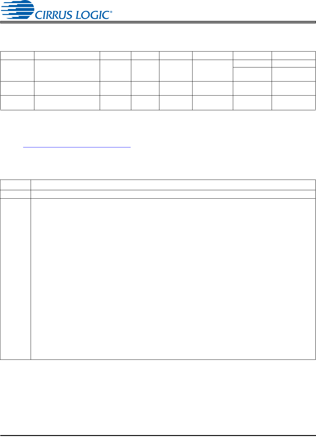
13.ORDERING INFORMATION
14.REFERENCES
1. Philips Semiconductor, The I²C-Bus Specification: Version 2.1, January 2000.
http://www.semiconductors.philips.com
.
15.REVISION HISTORY
Product Description Package Pb-Free Grade Temp Range Container Order #
CS42L52
Low-Power, Stereo
CODEC with Headphone
and Speaker Amps
40L-QFN Yes Commercial -40 to +85° C
Rail CS42L52-CNZ
Tape and Reel CS42L52-CNZR
CDB42L52
CS42L52 Evaluation
Board
- No - - - CDB42L52
CRD42L52
CS42L52 Reference
Design
- No - - - CRD42L52
Revision Changes
F1 Initial draft
F2
Removed the Automotive specification.
Added AD0 characteristics to “I/O Pin Characteristics” on page 10.
Added AD0 pin to Figure 1. Typical Connection Diagram on page 11.
Updated Note 6 on page 15.
Updated the V
IH
specification for VL = 1.8 V in “Digital Interface Specifications and Characteristics” on page 22.
Updated “PWM Outputs” on page 32 to exclude support of a 384x MCLK to LRCK ratio.
Added register commands for entering and exiting DSP 16-bit, 8 kHz Fs, SCLK = MCLK, master mode in section
“DSP Mode” on page 35.
Updated Section 4.9 “Recommended Power-up Sequence” on page 37.
Updated Section 4.10 “Recommended Power-Down Sequence” on page 37.
Added a description of the AD0 pin to “I²C Control” on page 38.
Added AD0 detail to Figure 20. Control Port Timing, I²C Write on page 38 and Figure 21. Control Port Timing, I²C
Read on page 39.
Updated the first paragraph in “Register Quick Reference” on page 40 to allow for data sheet-specified control-
writes to reserved registers.
Removed I²C address heading row from “Register Quick Reference” on page 40.
Updated notes in “Auto-Detect” on page 44.
Updated table in “Speed Mode” on page 45.
Added note 1 in “Freeze Registers” on page 52.
Updated notes in “Digital Soft Ramp” on page 53.
Added note 4 to “Digital Zero Cross” on page 53.
Added notes 1 and 2 for ALC configuration in “ALC Enable and Attack Rate (Address 2Ah)” on page 67.
Corrected the E2 scale in the package drawing in “Package Dimensions” on page 80.