
User Manual


Table Of Contents
- 1. Pin Descriptions
- 2. Typical Connection Diagram
- 3. Characteristic and Specifications
- Recommended Operating Conditions
- Absolute Maximum Ratings
- Analog Input Characteristics
- ADC Digital Filter Characteristics
- Analog Output Characteristics
- Analog Passthrough Characteristics
- PWM Output Characteristics
- Headphone Output Power Characteristics
- Line Output Voltage Level Characteristics
- Combined DAC Interpolation and onChip Analog FIlter Response
- Switching Specifications - Serial Port
- Switching Specifications - I²C Control Port
- DC Electrical Characteristics
- Digital Interface Specifications and Characteristics
- Power Consumption
- 4. Applications
- 4.1 Overview
- 4.2 Analog Inputs
- 4.3 Analog Outputs
- 4.4 Analog In to Analog Out Passthrough
- 4.5 PWM Outputs
- 4.6 Serial Port Clocking
- 4.7 Digital Interface Formats
- 4.8 Initialization
- 4.9 Recommended Power-up Sequence
- 4.10 Recommended Power-Down Sequence
- 4.11 Required Initialization Settings
- 4.12 Control Port Operation
- 5. Register Quick Reference
- 6. Register Description
- 6.1 Chip I.D. and Revision Register (Address 01h) (Read Only)
- 6.2 Power Control 1 (Address 02h)
- 6.3 Power Control 2 (Address 03h)
- 6.4 Power Control 3 (Address 04h)
- 6.5 Clocking Control (Address 05h)
- 6.6 Interface Control 1 (Address 06h)
- 6.7 Interface Control 2 (Address 07h)
- 6.8 Input x Select: ADCA and PGAA (Address 08h), ADCB and PGAB (Address 09h)
- 6.9 Analog and HPF Control (Address 0Ah)
- 6.10 ADC HPF Corner Frequency (Address 0Bh)
- 6.11 Misc. ADC Control (Address 0Ch)
- 6.12 Playback Control 1 (Address 0Dh)
- 6.13 Miscellaneous Controls (Address 0Eh)
- 6.14 Playback Control 2 (Address 0Fh)
- 6.15 MICx Amp Control:MIC A (Address 10h) and MIC B (Address 11h)
- 6.16 PGAx Vol. and ALCx Transition Ctl.: ALC, PGA A (Address 12h) and ALC, PGA B (Address 13h)
- 6.17 Passthrough x Volume: PASSAVOL (Address 14h) and PASSBVOL (Address 15h)
- 6.18 ADCx Volume Control: ADCAVOL (Address 16h) and ADCBVOL (Address 17h)
- 6.19 ADCx Mixer Volume: ADCA (Address 18h) and ADCB (Address 19h)
- 6.20 PCMx Mixer Volume: PCMA (Address 1Ah) and PCMB (Address 1Bh)
- 6.21 Beep Frequency and On Time (Address 1Ch)
- 6.22 Beep Volume and Off Time (Address 1Dh)
- 6.23 Beep and Tone Configuration (Address 1Eh)
- 6.24 Tone Control (Address 1Fh)
- 6.25 Master Volume Control: MSTA (Address 20h) and MSTB (Address 21h)
- 6.26 Headphone Volume Control: HPA (Address 22h) and HPB (Address 23h)
- 6.27 Speaker Volume Control: SPKA (Address 24h) and SPKB (Address 25h)
- 6.28 ADC and PCM Channel Mixer (Address 26h)
- 6.29 Limiter Control 1, Min/Max Thresholds (Address 27h)
- 6.30 Limiter Control 2, Release Rate (Address 28h)
- 6.31 Limiter Attack Rate (Address 29h)
- 6.32 ALC Enable and Attack Rate (Address 2Ah)
- 6.33 ALC Release Rate (Address 2Bh)
- 6.34 ALC Threshold (Address 2Ch)
- 6.35 Noise Gate Control (Address 2Dh)
- 6.36 Status (Address 2Eh) (Read Only)
- 6.37 Battery Compensation (Address 2Fh)
- 6.38 VP Battery Level (Address 30h) (Read Only)
- 6.39 Speaker Status (Address 31h) (Read Only)
- 6.40 Charge Pump Frequency (Address 34h)
- 7. Analog Performance Plots
- 8. Example System Clock Frequencies
- 9. PCB Layout Considerations
- 10. ADC and DAC Digital Filters
- 11. Parameter Definitions
- 12. Package Dimensions
- 13. Ordering Information
- 14. References
- 15. Revision History
8 DS680F2
CS42L52
3/1/13
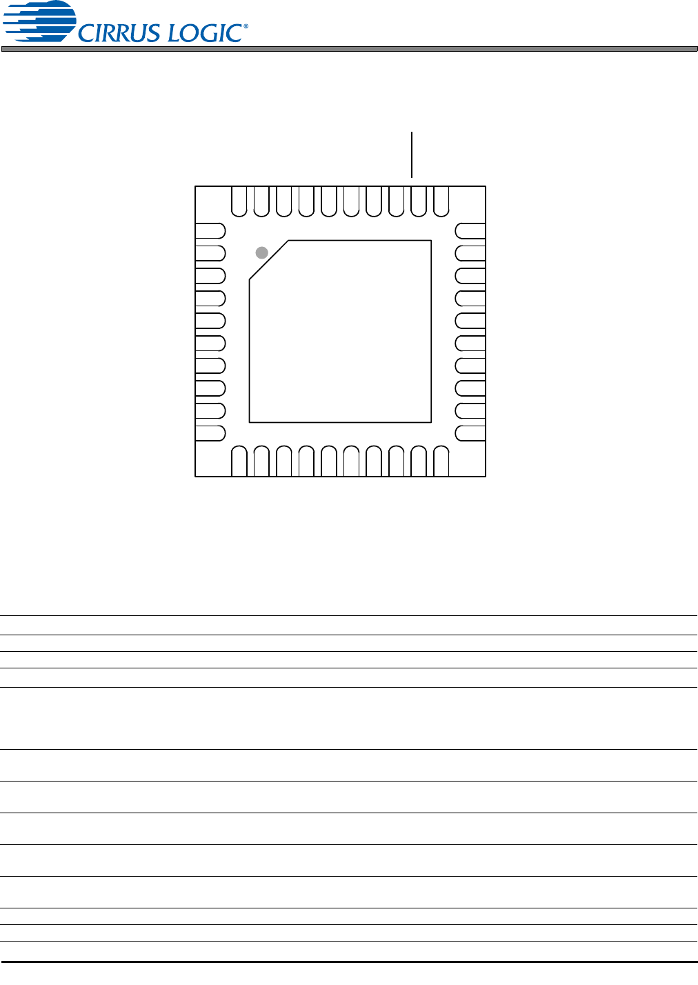
1. PIN DESCRIPTIONS
Pin Name # Pin Description
SDA 1 Serial Control Data (Input/Output) - SDA is a data I/O in I²C Mode.
SCL 2 Serial Control Port Clock (Input) - Serial clock for the serial control port.
AD0 3
Address Bit 0 (Input) - Chip address bit 0.
SPKR_OUTA+
SPKR_OUTA-
SPKR_OUTB+
SPKR_OUTB-
4
6
7
9
PWM Speaker Output (Output) - Full-bridge amplified PWM speaker outputs.
VP
5
8
Power for PWM Drivers (Input) - Power supply for the PWM output driver stages.
-VHPFILT 10
Inverting Charge Pump Filter Connection (Output) - Power supply from the inverting charge
pump that provides the negative rail for the headphone/line amplifiers.
FLYN 11
Charge Pump Cap Negative Node (Output) - Negative node for the inverting charge pump’s fly-
ing capacitor.
FLYP 12
Charge Pump Cap Positive Node (Output) - Positive node for the inverting charge pump’s flying
capacitor.
+VHP 13
Positive Analog Power for Headphone (Input) - Positive voltage rail and power for the internal
headphone amplifiers and inverting charge pump.
HP/LINE_OUTB, A 14,15 Headphone/Line Audio Output (Output) - Stereo headphone or line level analog outputs.
VA 16 Analog Power (Input) - Positive power for the internal analog section.
12
11
13
14
15
16
17
18
19
20
29
30
28
27
26
25
24
23
22
21
39
40
38
37
36
35
34
33
32
31
2
1
3
4
5
6
7
8
9
10
GND/Thermal Pad
SDOUT
MCLK
SCLK
SDIN
SDA
LRCK
FLYN
+VHP
HP/LINE_OUTB
HP/LINE_OUTA
VQ
MICBIAS
AIN4A/MIC1+/MIC2A
AIN2A
AD0
SPKR_OUTA+
VP
VP
VD
SPKR_OUTB-
-VHPFILT
AIN4B/MIC2+/MIC2B
AIN1B
AIN2B
AFILTB
AIN3B/MIC2-/MIC1B
AFILTA
AIN1A
AIN3A/MIC1-/MIC1A
SPKR_OUTB+
SCL
DGND
SPKR_OUTA-
FLYP
VA
AGND
FILT+
RESET
VL
SPKR/HP
Top-Down (Through-Package) View
40-Pin QFN Package