
User Manual


Table Of Contents
- 1. Pin Descriptions
- 2. Typical Connection Diagram
- 3. Characteristic and Specifications
- Recommended Operating Conditions
- Absolute Maximum Ratings
- Analog Input Characteristics
- ADC Digital Filter Characteristics
- Analog Output Characteristics
- Analog Passthrough Characteristics
- PWM Output Characteristics
- Headphone Output Power Characteristics
- Line Output Voltage Level Characteristics
- Combined DAC Interpolation and onChip Analog FIlter Response
- Switching Specifications - Serial Port
- Switching Specifications - I²C Control Port
- DC Electrical Characteristics
- Digital Interface Specifications and Characteristics
- Power Consumption
- 4. Applications
- 4.1 Overview
- 4.2 Analog Inputs
- 4.3 Analog Outputs
- 4.4 Analog In to Analog Out Passthrough
- 4.5 PWM Outputs
- 4.6 Serial Port Clocking
- 4.7 Digital Interface Formats
- 4.8 Initialization
- 4.9 Recommended Power-up Sequence
- 4.10 Recommended Power-Down Sequence
- 4.11 Required Initialization Settings
- 4.12 Control Port Operation
- 5. Register Quick Reference
- 6. Register Description
- 6.1 Chip I.D. and Revision Register (Address 01h) (Read Only)
- 6.2 Power Control 1 (Address 02h)
- 6.3 Power Control 2 (Address 03h)
- 6.4 Power Control 3 (Address 04h)
- 6.5 Clocking Control (Address 05h)
- 6.6 Interface Control 1 (Address 06h)
- 6.7 Interface Control 2 (Address 07h)
- 6.8 Input x Select: ADCA and PGAA (Address 08h), ADCB and PGAB (Address 09h)
- 6.9 Analog and HPF Control (Address 0Ah)
- 6.10 ADC HPF Corner Frequency (Address 0Bh)
- 6.11 Misc. ADC Control (Address 0Ch)
- 6.12 Playback Control 1 (Address 0Dh)
- 6.13 Miscellaneous Controls (Address 0Eh)
- 6.14 Playback Control 2 (Address 0Fh)
- 6.15 MICx Amp Control:MIC A (Address 10h) and MIC B (Address 11h)
- 6.16 PGAx Vol. and ALCx Transition Ctl.: ALC, PGA A (Address 12h) and ALC, PGA B (Address 13h)
- 6.17 Passthrough x Volume: PASSAVOL (Address 14h) and PASSBVOL (Address 15h)
- 6.18 ADCx Volume Control: ADCAVOL (Address 16h) and ADCBVOL (Address 17h)
- 6.19 ADCx Mixer Volume: ADCA (Address 18h) and ADCB (Address 19h)
- 6.20 PCMx Mixer Volume: PCMA (Address 1Ah) and PCMB (Address 1Bh)
- 6.21 Beep Frequency and On Time (Address 1Ch)
- 6.22 Beep Volume and Off Time (Address 1Dh)
- 6.23 Beep and Tone Configuration (Address 1Eh)
- 6.24 Tone Control (Address 1Fh)
- 6.25 Master Volume Control: MSTA (Address 20h) and MSTB (Address 21h)
- 6.26 Headphone Volume Control: HPA (Address 22h) and HPB (Address 23h)
- 6.27 Speaker Volume Control: SPKA (Address 24h) and SPKB (Address 25h)
- 6.28 ADC and PCM Channel Mixer (Address 26h)
- 6.29 Limiter Control 1, Min/Max Thresholds (Address 27h)
- 6.30 Limiter Control 2, Release Rate (Address 28h)
- 6.31 Limiter Attack Rate (Address 29h)
- 6.32 ALC Enable and Attack Rate (Address 2Ah)
- 6.33 ALC Release Rate (Address 2Bh)
- 6.34 ALC Threshold (Address 2Ch)
- 6.35 Noise Gate Control (Address 2Dh)
- 6.36 Status (Address 2Eh) (Read Only)
- 6.37 Battery Compensation (Address 2Fh)
- 6.38 VP Battery Level (Address 30h) (Read Only)
- 6.39 Speaker Status (Address 31h) (Read Only)
- 6.40 Charge Pump Frequency (Address 34h)
- 7. Analog Performance Plots
- 8. Example System Clock Frequencies
- 9. PCB Layout Considerations
- 10. ADC and DAC Digital Filters
- 11. Parameter Definitions
- 12. Package Dimensions
- 13. Ordering Information
- 14. References
- 15. Revision History
76 DS680F2
CS42L52
3/1/13
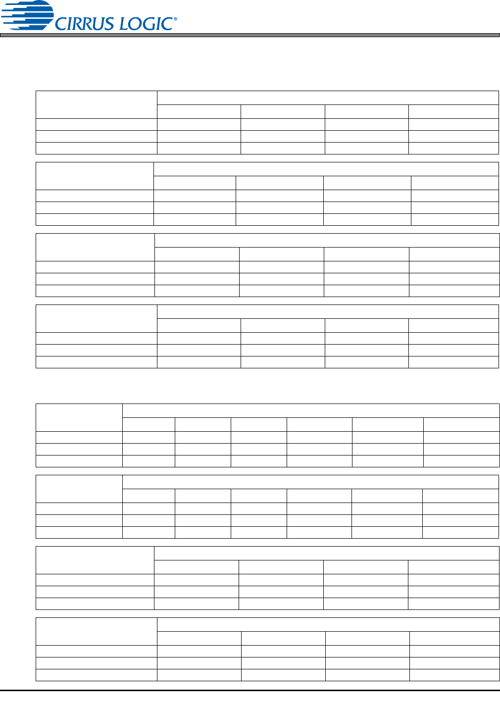
8. EXAMPLE SYSTEM CLOCK FREQUENCIES *The”MCLKDIV2” bit must be enabled.
8.1 Auto Detect Enabled
8.2 Auto Detect Disabled
Sample Rate
LRCK (kHz)
MCLK (MHz)
1024x 1536x 2048x* 3072x*
8 8.1920 12.2880 16.3840 24.5760
11.025 11.2896 16.9344 22.5792 33.8688
12 12.2880 18.4320 24.5760 36.8640
Sample Rate
LRCK (kHz)
MCLK (MHz)
512x 768x 1024x* 1536x*
16 8.1920 12.2880 16.3840 24.5760
22.05 11.2896 16.9344 22.5792 33.8688
24 12.2880 18.4320 24.5760 36.8640
Sample Rate
LRCK (kHz)
MCLK (MHz)
256x 384x 512x* 768x*
32 8.1920 12.2880 16.3840 24.5760
44.1 11.2896 16.9344 22.5792 33.8688
48 12.2880 18.4320 24.5760 36.8640
Sample Rate
LRCK (kHz)
MCLK (MHz)
128x 192x 256x* 384x*
64 8.1920 12.2880 16.3840 24.5760
88.2 11.2896 16.9344 22.5792 33.8688
96 12.2880 18.4320 24.5760 36.8640
Sample Rate
LRCK (kHz)
MCLK (MHz)
512x 768x 1024x 1536x 2048x 3072x
8 - 6.1440 8.1920 12.2880 16.3840 24.5760
11.025 - 8.4672 11.2896 16.9344 22.5792 33.8688
12 6.1440 9.2160 12.2880 18.4320 24.5760 36.8640
Sample Rate
LRCK (kHz)
MCLK (MHz)
256x 384x 512x 768x 1024x 1536x
16 - 6.1440 8.1920 12.2880 16.3840 24.5760
22.05 - 8.4672 11.2896 16.9344 22.5792 33.8688
24 6.1440 9.2160 12.2880 18.4320 24.5760 36.8640
Sample Rate
LRCK (kHz)
MCLK (MHz)
256x 384x 512x 768x
32 8.1920 12.2880 16.3840 24.5760
44.1 11.2896 16.9344 22.5792 33.8688
48 12.2880 18.4320 24.5760 36.8640
Sample Rate
LRCK (kHz)
MCLK (MHz)
128x 192x 256x 384x
64 8.1920 12.2880 16.3840 24.5760
88.2 11.2896 16.9344 22.5792 33.8688
96 12.2880 18.4320 24.5760 36.8640