
User Manual
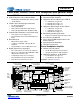


Table Of Contents
- 1. Pin Descriptions
- 2. Typical Connection Diagram
- 3. Characteristic and Specifications
- Recommended Operating Conditions
- Absolute Maximum Ratings
- Analog Input Characteristics
- ADC Digital Filter Characteristics
- Analog Output Characteristics
- Analog Passthrough Characteristics
- PWM Output Characteristics
- Headphone Output Power Characteristics
- Line Output Voltage Level Characteristics
- Combined DAC Interpolation and onChip Analog FIlter Response
- Switching Specifications - Serial Port
- Switching Specifications - I²C Control Port
- DC Electrical Characteristics
- Digital Interface Specifications and Characteristics
- Power Consumption
- 4. Applications
- 4.1 Overview
- 4.2 Analog Inputs
- 4.3 Analog Outputs
- 4.4 Analog In to Analog Out Passthrough
- 4.5 PWM Outputs
- 4.6 Serial Port Clocking
- 4.7 Digital Interface Formats
- 4.8 Initialization
- 4.9 Recommended Power-up Sequence
- 4.10 Recommended Power-Down Sequence
- 4.11 Required Initialization Settings
- 4.12 Control Port Operation
- 5. Register Quick Reference
- 6. Register Description
- 6.1 Chip I.D. and Revision Register (Address 01h) (Read Only)
- 6.2 Power Control 1 (Address 02h)
- 6.3 Power Control 2 (Address 03h)
- 6.4 Power Control 3 (Address 04h)
- 6.5 Clocking Control (Address 05h)
- 6.6 Interface Control 1 (Address 06h)
- 6.7 Interface Control 2 (Address 07h)
- 6.8 Input x Select: ADCA and PGAA (Address 08h), ADCB and PGAB (Address 09h)
- 6.9 Analog and HPF Control (Address 0Ah)
- 6.10 ADC HPF Corner Frequency (Address 0Bh)
- 6.11 Misc. ADC Control (Address 0Ch)
- 6.12 Playback Control 1 (Address 0Dh)
- 6.13 Miscellaneous Controls (Address 0Eh)
- 6.14 Playback Control 2 (Address 0Fh)
- 6.15 MICx Amp Control:MIC A (Address 10h) and MIC B (Address 11h)
- 6.16 PGAx Vol. and ALCx Transition Ctl.: ALC, PGA A (Address 12h) and ALC, PGA B (Address 13h)
- 6.17 Passthrough x Volume: PASSAVOL (Address 14h) and PASSBVOL (Address 15h)
- 6.18 ADCx Volume Control: ADCAVOL (Address 16h) and ADCBVOL (Address 17h)
- 6.19 ADCx Mixer Volume: ADCA (Address 18h) and ADCB (Address 19h)
- 6.20 PCMx Mixer Volume: PCMA (Address 1Ah) and PCMB (Address 1Bh)
- 6.21 Beep Frequency and On Time (Address 1Ch)
- 6.22 Beep Volume and Off Time (Address 1Dh)
- 6.23 Beep and Tone Configuration (Address 1Eh)
- 6.24 Tone Control (Address 1Fh)
- 6.25 Master Volume Control: MSTA (Address 20h) and MSTB (Address 21h)
- 6.26 Headphone Volume Control: HPA (Address 22h) and HPB (Address 23h)
- 6.27 Speaker Volume Control: SPKA (Address 24h) and SPKB (Address 25h)
- 6.28 ADC and PCM Channel Mixer (Address 26h)
- 6.29 Limiter Control 1, Min/Max Thresholds (Address 27h)
- 6.30 Limiter Control 2, Release Rate (Address 28h)
- 6.31 Limiter Attack Rate (Address 29h)
- 6.32 ALC Enable and Attack Rate (Address 2Ah)
- 6.33 ALC Release Rate (Address 2Bh)
- 6.34 ALC Threshold (Address 2Ch)
- 6.35 Noise Gate Control (Address 2Dh)
- 6.36 Status (Address 2Eh) (Read Only)
- 6.37 Battery Compensation (Address 2Fh)
- 6.38 VP Battery Level (Address 30h) (Read Only)
- 6.39 Speaker Status (Address 31h) (Read Only)
- 6.40 Charge Pump Frequency (Address 34h)
- 7. Analog Performance Plots
- 8. Example System Clock Frequencies
- 9. PCB Layout Considerations
- 10. ADC and DAC Digital Filters
- 11. Parameter Definitions
- 12. Package Dimensions
- 13. Ordering Information
- 14. References
- 15. Revision History
DS680F2 7
CS42L52
3/1/13
9.1 Power Supply and Grounding ......................................................................................................... 77
9.2 QFN Thermal Pad .......................................................................................................................... 77
10. ADC AND DAC DIGITAL FILTERS .................................................................................................. 78
11. PARAMETER DEFINITIONS .............................................................................................................. 79
12. PACKAGE DIMENSIONS .................................................................................................................. 80
THERMAL CHARACTERISTICS .......................................................................................................... 80
13. ORDERING INFORMATION .............................................................................................................. 81
14. REFERENCES .................................................................................................................................... 81
15. REVISION HISTORY .......................................................................................................................... 81
LIST OF TABLES
Table 1. MCLK, LRCK Quick Decode ....................................................................................................... 34
LIST OF FIGURES
Figure 1. Typical Connection Diagram ...................................................................................................... 11
Figure 2. Headphone Output Test Load .................................................................................................... 18
Figure 3. Serial Audio Interface Timing ..................................................................................................... 20
Figure 4. Control Port Timing - I²C ............................................................................................................ 21
Figure 5. Analog Input Signal Flow ........................................................................................................... 25
Figure 6. Single-Ended MIC Configuration ............................................................................................... 26
Figure 7. Differential MIC Configuration .................................................................................................... 26
Figure 8. ALC ............................................................................................................................................ 27
Figure 9. Noise Gate Attenuation .............................................................................................................. 27
Figure 10. DSP Engine Signal Flow .......................................................................................................... 28
Figure 11. PWM Output Stage .................................................................................................................. 29
Figure 12. Analog Output Stage ................................................................................................................ 29
Figure 13. Beep Configuration Options ..................................................................................................... 30
Figure 14. Peak Detect and Limiter ........................................................................................................... 31
Figure 15. Battery Compensation ............................................................................................................. 33
Figure 16. I²S Format ................................................................................................................................ 35
Figure 17. Left-Justified Format ................................................................................................................ 35
Figure 18. Right-Justified Format (DAC only) ........................................................................................... 35
Figure 19. DSP Mode Format) .................................................................................................................. 36
Figure 20. Control Port Timing, I²C Write .................................................................................................. 38
Figure 21. Control Port Timing, I²C Read .................................................................................................. 39
Figure 22. THD+N vs. Output Power per Channel at 1.8 V (16 load) ................................................... 74
Figure 23. THD+N vs. Output Power per Channel at 2.5 V (16 load) ................................................... 74
Figure 24. THD+N vs. Output Power per Channel at 1.8 V (32 load) ................................................... 75
Figure 25. THD+N vs. Output Power per Channel at 2.5 V (32 load) ................................................... 75
Figure 26. ADC Passband Ripple ............................................................................................................. 78
Figure 27. ADC Stopband Rejection ......................................................................................................... 78
Figure 28. ADC Transition Band ............................................................................................................... 78
Figure 29. ADC Transition Band (Detail) ................................................................................................... 78
Figure 30. DAC Passband Ripple ............................................................................................................. 78
Figure 31. DAC Stopband ......................................................................................................................... 78
Figure 32. DAC Transition Band ............................................................................................................... 78
Figure 33. DAC Transition Band (Detail) ................................................................................................... 78