
User Manual


Table Of Contents
- 1. Pin Descriptions
- 2. Typical Connection Diagram
- 3. Characteristic and Specifications
- Recommended Operating Conditions
- Absolute Maximum Ratings
- Analog Input Characteristics
- ADC Digital Filter Characteristics
- Analog Output Characteristics
- Analog Passthrough Characteristics
- PWM Output Characteristics
- Headphone Output Power Characteristics
- Line Output Voltage Level Characteristics
- Combined DAC Interpolation and onChip Analog FIlter Response
- Switching Specifications - Serial Port
- Switching Specifications - I²C Control Port
- DC Electrical Characteristics
- Digital Interface Specifications and Characteristics
- Power Consumption
- 4. Applications
- 4.1 Overview
- 4.2 Analog Inputs
- 4.3 Analog Outputs
- 4.4 Analog In to Analog Out Passthrough
- 4.5 PWM Outputs
- 4.6 Serial Port Clocking
- 4.7 Digital Interface Formats
- 4.8 Initialization
- 4.9 Recommended Power-up Sequence
- 4.10 Recommended Power-Down Sequence
- 4.11 Required Initialization Settings
- 4.12 Control Port Operation
- 5. Register Quick Reference
- 6. Register Description
- 6.1 Chip I.D. and Revision Register (Address 01h) (Read Only)
- 6.2 Power Control 1 (Address 02h)
- 6.3 Power Control 2 (Address 03h)
- 6.4 Power Control 3 (Address 04h)
- 6.5 Clocking Control (Address 05h)
- 6.6 Interface Control 1 (Address 06h)
- 6.7 Interface Control 2 (Address 07h)
- 6.8 Input x Select: ADCA and PGAA (Address 08h), ADCB and PGAB (Address 09h)
- 6.9 Analog and HPF Control (Address 0Ah)
- 6.10 ADC HPF Corner Frequency (Address 0Bh)
- 6.11 Misc. ADC Control (Address 0Ch)
- 6.12 Playback Control 1 (Address 0Dh)
- 6.13 Miscellaneous Controls (Address 0Eh)
- 6.14 Playback Control 2 (Address 0Fh)
- 6.15 MICx Amp Control:MIC A (Address 10h) and MIC B (Address 11h)
- 6.16 PGAx Vol. and ALCx Transition Ctl.: ALC, PGA A (Address 12h) and ALC, PGA B (Address 13h)
- 6.17 Passthrough x Volume: PASSAVOL (Address 14h) and PASSBVOL (Address 15h)
- 6.18 ADCx Volume Control: ADCAVOL (Address 16h) and ADCBVOL (Address 17h)
- 6.19 ADCx Mixer Volume: ADCA (Address 18h) and ADCB (Address 19h)
- 6.20 PCMx Mixer Volume: PCMA (Address 1Ah) and PCMB (Address 1Bh)
- 6.21 Beep Frequency and On Time (Address 1Ch)
- 6.22 Beep Volume and Off Time (Address 1Dh)
- 6.23 Beep and Tone Configuration (Address 1Eh)
- 6.24 Tone Control (Address 1Fh)
- 6.25 Master Volume Control: MSTA (Address 20h) and MSTB (Address 21h)
- 6.26 Headphone Volume Control: HPA (Address 22h) and HPB (Address 23h)
- 6.27 Speaker Volume Control: SPKA (Address 24h) and SPKB (Address 25h)
- 6.28 ADC and PCM Channel Mixer (Address 26h)
- 6.29 Limiter Control 1, Min/Max Thresholds (Address 27h)
- 6.30 Limiter Control 2, Release Rate (Address 28h)
- 6.31 Limiter Attack Rate (Address 29h)
- 6.32 ALC Enable and Attack Rate (Address 2Ah)
- 6.33 ALC Release Rate (Address 2Bh)
- 6.34 ALC Threshold (Address 2Ch)
- 6.35 Noise Gate Control (Address 2Dh)
- 6.36 Status (Address 2Eh) (Read Only)
- 6.37 Battery Compensation (Address 2Fh)
- 6.38 VP Battery Level (Address 30h) (Read Only)
- 6.39 Speaker Status (Address 31h) (Read Only)
- 6.40 Charge Pump Frequency (Address 34h)
- 7. Analog Performance Plots
- 8. Example System Clock Frequencies
- 9. PCB Layout Considerations
- 10. ADC and DAC Digital Filters
- 11. Parameter Definitions
- 12. Package Dimensions
- 13. Ordering Information
- 14. References
- 15. Revision History
DS680F2 41
CS42L52
3/1/13
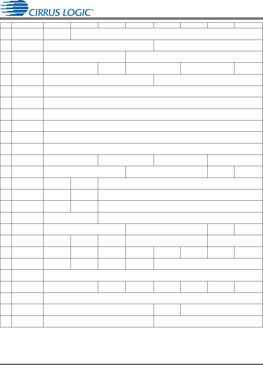
1Bh PCMMIXB Vol PMIXBMUTE PMIXBVOL6 PMIXBVOL5 PMIXBVOL4 PMIXBVOL3 PMIXBVOL2 PMIXBVOL1 PMIXBVOL0
p58 00 0 0 000 0
1Ch BEEP Freq,
On Time
FREQ3 FREQ2 FREQ1 FREQ0 ONTIME3 ONTIME2 ONTIME1 ONTIME0
p59 00 0 0 000 0
1Dh BEEP Vol,
Off Time
OFFTIME2 OFFTIME1 OFFTIME0 BPVOL4 BPVOL3 BPVOL2 BPVOL1 BPVOL0
p60 00 0 0 000 0
1Eh BEEP,
Tone Cfg.
BEEP1 BEEP0 BEEPMIXDIS TREB_CF1 TREB_CF0 BASS_CF1 BASS_CF0 TC_EN
p61 00 0 0 000 0
1Fh Tone Ctl TREB3 TREB2 TREB1 TREB0 BASS3 BASS2 BASS1 BASS0
p62 10 0 0 100 0
20h Master A Vol MSTAVOL7 MSTAVOL6 MSTAVOL5 MSTAVOL4 MSTAVOL3 MSTAVOL2 MSTAVOL1 MSTAVOL0
p63 00 0 0 000 0
21h Master B Vol MSTBVOL7 MSTBVOL6 MSTBVOL5 MSTBVOL4 MSTBVOL3 MSTBVOL2 MSTBVOL1 MSTBVOL0
p63 00 0 0 000 0
22h Headphone A
Volume
HPAVOL7 HPAVOL6 HPAVOL5 HPAVOL4 HPAVOL3 HPAVOL2 HPAVOL1 HPAVOL0
p63 00 0 0 000 0
23h Headphone B
Volume
HPBVOL7 HPBVOL6 HPBVOL5 HPBVOL4 HPBVOL3 HPBVOL2 HPBVOL1 HPBVOL0
p63 00 0 0 000 0
24h Speaker A
Volume
SPKAVOL7 SPKAVOL6 SPKAVOL5 SPKAVOL4 SPKAVOL3 SPKAVOL2 SPKAVOL1 SPKAVOL0
p64 00 0 0 000 0
25h Speaker B
Volume
SPKBVOL7 SPKBVOL6 SPKBVOL5 SPKBVOL4 SPKBVOL3 SPKBVOL2 SPKBVOL1 SPKBVOL0
p64 00 0 0 000 0
26h Channel Mixer
and Swap
PCMASWP1 PCMASWP0 PCMBSWP1 PCMBSWP0 ADCASWP1 ADCASWP0 ADCBSWP1 ADCBSWP0
p64 00 0 0 000 0
27h Limit Ctl 1,
Thresholds
LMAX2 LMAX1 LMAX0 CUSH2 CUSH1 CUSH0 LIMSRDIS LIMZCDIS
p65 00 0 0 000 0
28h Limit Ctl 2,
Release Rate
LIMIT LIMIT_ALL LIMRRATE5 LIMRRATE4 LIMRRATE3 LIMRRATE2 LIMRRATE1 LIMRRATE0
p66 01 1 1 111 1
29h Limiter Attack
Rate
Reserved Reserved LIMARATE5 LIMARATE4 LIMARATE3 LIMARATE2 LIMARATE1 LIMARATE0
p67 11 0 0 000 0
2Ah ALC Ctl 1,
Attack Rate
ALCB ALCA ALCARATE5 AALCRATE4 ALCARATE3 ALCARATE2 ALCARATE1 ALCARATE0
p67 00 0 0 000 0
2Bh ALC Release
Rate
Reserved Reserved ALCRRATE5 ALCRRATE4 ALCRRATE3 ALCRRATE2 ALCRRATE1 ALCRRATE0
p68 00 1 1 111 1
2Ch ALC Thresh-
olds
ALCMAX2 ALCMAX1 ALCMAX0 ALCMIN2 ALCMIN1 ALCMIN0 Reserved Reserved
p68 00 0 0 000 0
2Dh Noise Gate Ctl NGALL NG NGBOOST THRESH2 THRESH1 THRESH0 NGDELAY1 NGDELAY0
p69 00 0 0 000 0
2Eh Overflow and
Clock Status
Reserved SPCLKERR DSPBOVFL DSPAOVFL PCMAOVFL PCMBOVFL ADCAOVFL ADCBOVFL
p70 00 0 0 000 0
2Fh Battery Com-
pensation
BATTCMP VPMONITOR Reserved Reserved VPREF3 VPREF2 VPREF1 VPREF0
p71 00 0 0 000 0
30h VP Battery
Level
VPLVL7 VPLVL6 VPLVL5 VPLVL4 VPLVL3 VPLVL2 VPLVL1 VPLVL0
p72 00 0 0 000 0
31h Speaker Status Reserved Reserved SPKASHRT SPKBSHRT SPKR/HP Reserved Reserved Reserved
p72 00 0 0 000 0
32h Reserved Reserved Reserved Reserved Reserved Reserved Reserved Reserved Reserved
00 1 1 101 1
33h Reserved Reserved Reserved Reserved Reserved Reserved Reserved Reserved Reserved
00 0 0 000 0
34h Charge Pump
Frequency
CHGFREQ3 CHGFREQ2 CHGFREQ1 CHGFREQ0 Reserved Reserved Reserved Reserved
p73 01 0 1 111 1
Adr. Function 7 6 5 4 3 2 1 0