
User Manual


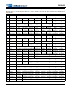
Table Of Contents
- 1. Pin Descriptions
- 2. Typical Connection Diagram
- 3. Characteristic and Specifications
- Recommended Operating Conditions
- Absolute Maximum Ratings
- Analog Input Characteristics
- ADC Digital Filter Characteristics
- Analog Output Characteristics
- Analog Passthrough Characteristics
- PWM Output Characteristics
- Headphone Output Power Characteristics
- Line Output Voltage Level Characteristics
- Combined DAC Interpolation and onChip Analog FIlter Response
- Switching Specifications - Serial Port
- Switching Specifications - I²C Control Port
- DC Electrical Characteristics
- Digital Interface Specifications and Characteristics
- Power Consumption
- 4. Applications
- 4.1 Overview
- 4.2 Analog Inputs
- 4.3 Analog Outputs
- 4.4 Analog In to Analog Out Passthrough
- 4.5 PWM Outputs
- 4.6 Serial Port Clocking
- 4.7 Digital Interface Formats
- 4.8 Initialization
- 4.9 Recommended Power-up Sequence
- 4.10 Recommended Power-Down Sequence
- 4.11 Required Initialization Settings
- 4.12 Control Port Operation
- 5. Register Quick Reference
- 6. Register Description
- 6.1 Chip I.D. and Revision Register (Address 01h) (Read Only)
- 6.2 Power Control 1 (Address 02h)
- 6.3 Power Control 2 (Address 03h)
- 6.4 Power Control 3 (Address 04h)
- 6.5 Clocking Control (Address 05h)
- 6.6 Interface Control 1 (Address 06h)
- 6.7 Interface Control 2 (Address 07h)
- 6.8 Input x Select: ADCA and PGAA (Address 08h), ADCB and PGAB (Address 09h)
- 6.9 Analog and HPF Control (Address 0Ah)
- 6.10 ADC HPF Corner Frequency (Address 0Bh)
- 6.11 Misc. ADC Control (Address 0Ch)
- 6.12 Playback Control 1 (Address 0Dh)
- 6.13 Miscellaneous Controls (Address 0Eh)
- 6.14 Playback Control 2 (Address 0Fh)
- 6.15 MICx Amp Control:MIC A (Address 10h) and MIC B (Address 11h)
- 6.16 PGAx Vol. and ALCx Transition Ctl.: ALC, PGA A (Address 12h) and ALC, PGA B (Address 13h)
- 6.17 Passthrough x Volume: PASSAVOL (Address 14h) and PASSBVOL (Address 15h)
- 6.18 ADCx Volume Control: ADCAVOL (Address 16h) and ADCBVOL (Address 17h)
- 6.19 ADCx Mixer Volume: ADCA (Address 18h) and ADCB (Address 19h)
- 6.20 PCMx Mixer Volume: PCMA (Address 1Ah) and PCMB (Address 1Bh)
- 6.21 Beep Frequency and On Time (Address 1Ch)
- 6.22 Beep Volume and Off Time (Address 1Dh)
- 6.23 Beep and Tone Configuration (Address 1Eh)
- 6.24 Tone Control (Address 1Fh)
- 6.25 Master Volume Control: MSTA (Address 20h) and MSTB (Address 21h)
- 6.26 Headphone Volume Control: HPA (Address 22h) and HPB (Address 23h)
- 6.27 Speaker Volume Control: SPKA (Address 24h) and SPKB (Address 25h)
- 6.28 ADC and PCM Channel Mixer (Address 26h)
- 6.29 Limiter Control 1, Min/Max Thresholds (Address 27h)
- 6.30 Limiter Control 2, Release Rate (Address 28h)
- 6.31 Limiter Attack Rate (Address 29h)
- 6.32 ALC Enable and Attack Rate (Address 2Ah)
- 6.33 ALC Release Rate (Address 2Bh)
- 6.34 ALC Threshold (Address 2Ch)
- 6.35 Noise Gate Control (Address 2Dh)
- 6.36 Status (Address 2Eh) (Read Only)
- 6.37 Battery Compensation (Address 2Fh)
- 6.38 VP Battery Level (Address 30h) (Read Only)
- 6.39 Speaker Status (Address 31h) (Read Only)
- 6.40 Charge Pump Frequency (Address 34h)
- 7. Analog Performance Plots
- 8. Example System Clock Frequencies
- 9. PCB Layout Considerations
- 10. ADC and DAC Digital Filters
- 11. Parameter Definitions
- 12. Package Dimensions
- 13. Ordering Information
- 14. References
- 15. Revision History
DS680F2 37
CS42L52
3/1/13
4.9 Recommended Power-up Sequence
1. Hold RESET low until the power supplies are stable.
2. Bring RESET
high.
3. The default state of the PDN bit is 1. Load the desired register settings while keeping the PDN bit set
to 11.
4. Load the required initialization settings listed in Section 4.11.
5. Apply MCLK at the appropriate frequency, as discussed in Section 4.6. SCLK may be applied or set to
master at any time; LRCK may only be applied or set to master while the PDN bit is set to 1.
6. Set the PDN bit to 0.
7. Bring RESET
low if the analog or digital supplies drop below the recommended operating condition to
prevent power glitch related issues.
4.10 Recommended Power-Down Sequence
To minimize audible pops when turning off or placing the CODEC in standby:
1. Mute the DACs, PWM outputs and ADCs.
2. Disable soft ramp and zero cross volume transitions.
3. Set the PDN bit to 1.
4. Wait at least 100 µs.
The CODEC will be fully powered down after this 100 µs delay. Prior to the removal of the master clock
(MCLK), this delay of at least 100 µs must be implemented after step 3 to avoid premature disruption
of the CODEC’s power down sequence.
A disruption in the CODEC’s power down sequence (i.e. removing the MCLK signal before this 100 µs
delay) has consequences on both the headphone and speaker amplifiers: The charge pump may stop
abruptly, causing the headphone amplifiers to drive the outputs up to the +VHP supply. Also, the last
state of each ‘+’ and ‘-’ PWM output terminal before the premature removal of MCLK could randomly
be held at either VP or AGND. When this event occurs, it is possible for each PWM terminal to output
opposing potentials, creating a DC source into the speaker voice coil.
The disruption of the CODEC’s power down sequence may also cause clicks and pops on the output
of the DACs as the modulator holds the last output level before the MCLK signal was removed.
5. Optionally, MCLK may be removed at this time.
6. To achieve the lowest operating quiescent current, bring RESET
low. All control port registers will be
reset to their default state.
7. Power Supply Removal (Option 1): Switch power supplies to a high impedance state.
8. Power Supply Removal (Option 2): To minimize pops when the power supplies are pulled to ground, a
discharge resistor must be added in parallel with the capacitor on the FILT+ pin. With a 1 M resistor
and a 2.2 µF capacitor on FILT+, FILT+ will ramp to ground in approximately 5 seconds. A 1 M resistor
on FILT+ reduces the full scale input/output voltage by approximately 0.25 dB.
After step 5, wait the required time for FILT+ to ramp to ground before pulling VA to ground.
4.11 Required Initialization Settings
The current and thresholds required for various sections in the CODEC must be adjusted by implementing
the initialization settings shown below after power-up sequence step 3. All performance and power con-
sumption measurements were taken with the following settings: