
User Manual


Table Of Contents
- 1. Pin Descriptions
- 2. Typical Connection Diagram
- 3. Characteristic and Specifications
- Recommended Operating Conditions
- Absolute Maximum Ratings
- Analog Input Characteristics
- ADC Digital Filter Characteristics
- Analog Output Characteristics
- Analog Passthrough Characteristics
- PWM Output Characteristics
- Headphone Output Power Characteristics
- Line Output Voltage Level Characteristics
- Combined DAC Interpolation and onChip Analog FIlter Response
- Switching Specifications - Serial Port
- Switching Specifications - I²C Control Port
- DC Electrical Characteristics
- Digital Interface Specifications and Characteristics
- Power Consumption
- 4. Applications
- 4.1 Overview
- 4.2 Analog Inputs
- 4.3 Analog Outputs
- 4.4 Analog In to Analog Out Passthrough
- 4.5 PWM Outputs
- 4.6 Serial Port Clocking
- 4.7 Digital Interface Formats
- 4.8 Initialization
- 4.9 Recommended Power-up Sequence
- 4.10 Recommended Power-Down Sequence
- 4.11 Required Initialization Settings
- 4.12 Control Port Operation
- 5. Register Quick Reference
- 6. Register Description
- 6.1 Chip I.D. and Revision Register (Address 01h) (Read Only)
- 6.2 Power Control 1 (Address 02h)
- 6.3 Power Control 2 (Address 03h)
- 6.4 Power Control 3 (Address 04h)
- 6.5 Clocking Control (Address 05h)
- 6.6 Interface Control 1 (Address 06h)
- 6.7 Interface Control 2 (Address 07h)
- 6.8 Input x Select: ADCA and PGAA (Address 08h), ADCB and PGAB (Address 09h)
- 6.9 Analog and HPF Control (Address 0Ah)
- 6.10 ADC HPF Corner Frequency (Address 0Bh)
- 6.11 Misc. ADC Control (Address 0Ch)
- 6.12 Playback Control 1 (Address 0Dh)
- 6.13 Miscellaneous Controls (Address 0Eh)
- 6.14 Playback Control 2 (Address 0Fh)
- 6.15 MICx Amp Control:MIC A (Address 10h) and MIC B (Address 11h)
- 6.16 PGAx Vol. and ALCx Transition Ctl.: ALC, PGA A (Address 12h) and ALC, PGA B (Address 13h)
- 6.17 Passthrough x Volume: PASSAVOL (Address 14h) and PASSBVOL (Address 15h)
- 6.18 ADCx Volume Control: ADCAVOL (Address 16h) and ADCBVOL (Address 17h)
- 6.19 ADCx Mixer Volume: ADCA (Address 18h) and ADCB (Address 19h)
- 6.20 PCMx Mixer Volume: PCMA (Address 1Ah) and PCMB (Address 1Bh)
- 6.21 Beep Frequency and On Time (Address 1Ch)
- 6.22 Beep Volume and Off Time (Address 1Dh)
- 6.23 Beep and Tone Configuration (Address 1Eh)
- 6.24 Tone Control (Address 1Fh)
- 6.25 Master Volume Control: MSTA (Address 20h) and MSTB (Address 21h)
- 6.26 Headphone Volume Control: HPA (Address 22h) and HPB (Address 23h)
- 6.27 Speaker Volume Control: SPKA (Address 24h) and SPKB (Address 25h)
- 6.28 ADC and PCM Channel Mixer (Address 26h)
- 6.29 Limiter Control 1, Min/Max Thresholds (Address 27h)
- 6.30 Limiter Control 2, Release Rate (Address 28h)
- 6.31 Limiter Attack Rate (Address 29h)
- 6.32 ALC Enable and Attack Rate (Address 2Ah)
- 6.33 ALC Release Rate (Address 2Bh)
- 6.34 ALC Threshold (Address 2Ch)
- 6.35 Noise Gate Control (Address 2Dh)
- 6.36 Status (Address 2Eh) (Read Only)
- 6.37 Battery Compensation (Address 2Fh)
- 6.38 VP Battery Level (Address 30h) (Read Only)
- 6.39 Speaker Status (Address 31h) (Read Only)
- 6.40 Charge Pump Frequency (Address 34h)
- 7. Analog Performance Plots
- 8. Example System Clock Frequencies
- 9. PCB Layout Considerations
- 10. ADC and DAC Digital Filters
- 11. Parameter Definitions
- 12. Package Dimensions
- 13. Ordering Information
- 14. References
- 15. Revision History
36 DS680F2
CS42L52
3/1/13
When configuring the 16-bit SDOUT word length with an 8 kHz sample rate in master mode and when
SCLK is set equal to MCLK, perform the following write sequences:
Register commands ONLY when entering DSP 16-bit, 8 kHz Fs, SCLK=MCLK, master mode:
Register commands when exiting DSP 16-bit, 8 kHz Fs, SCLK=MCLK, master mode:
4.8 Initialization
The CODEC enters a Power-down state on initial power-up. The interpolation and decimation filters, delta-
sigma and PWM modulators, and control port registers are reset. The internal voltage reference, and
switched-capacitor low-pass filters are powered down.
The device remains in Power-down state until the RESET
pin is brought high. The control port is accessible
once RESET
is high and the desired register settings can be loaded per the descriptions in the Section 6.
Once MCLK is valid, the quiescent voltage, VQ, and the internal voltage reference, FILT+, will begin power-
ing up to normal operation. The charge pump slowly powers up and charges the capacitors. Power is then
applied to the headphone amplifiers and switched-capacitor filters, and the analog/digital outputs enter a mut-
ed state. Once LRCK is valid, MCLK occurrences are counted over one LRCK period to determine the MC-
LK/LRCK frequency ratio and normal operation begins.
Register[Bits] Value Description
1 0x0C[1:0] 0x03 Mute the ADC outputs to ensure no audible artifacts are transmitted when changing modes.
2 Refer to Section 4.10 Follow the recommended power down sequence for the HP and PWM outputs.
3 0x02[0] 0x01 Power down the CODEC.
4 0x05[7:0] 0x72 Enable 8 kHz Fs for MCLK=12.000 MHz.
5 0x06[7:0] 0x93 Enable DSP 16-bit master mode.
6 0x07[6] 0x01 Enable SCLK=MCLK.
7 0x33[6] 0x01 Undisclosed register command for enabling mode mentioned above.
8 Refer to Section 4.9 Follow the recommended power up sequence for the HP and PWM outputs.
9 0x02[0] 0x00 Power up the CODEC.
10 0x0C[1:0] 0x00 Unmute the ADC outputs.
Register[Bits] Value Description
1 0x0C[1:0] 0x03 Mute the ADC outputs to ensure no audible artifacts are transmitted when changing modes.
2 Refer to Section 4.10 Follow the recommended power down sequence for the HP and PWM outputs.
3 0x02[0] 0x01 Power down the CODEC.
4 0x05[7:0] 0x20 Enable 48 kHz Fs for MCLK = 12.2880 MHz or re-establish original settings.
5 0x06[7:0] 0x00 Enable Left-Justified 24-bit slave mode or re-establish original settings.
6 0x07[6] 0x00 Disable SCLK=MCLK or re-establish original settings.
7 0x33[6] 0x00 Undisclosed register command for disabling mode mentioned above.
8 Refer to Section 4.9 Follow the recommended power up sequence for the HP and PWM outputs.
9 0x02[0] 0x00 Power up the CODEC.
10 0x0C[1:0] 0x00 Unmute the ADC outputs.
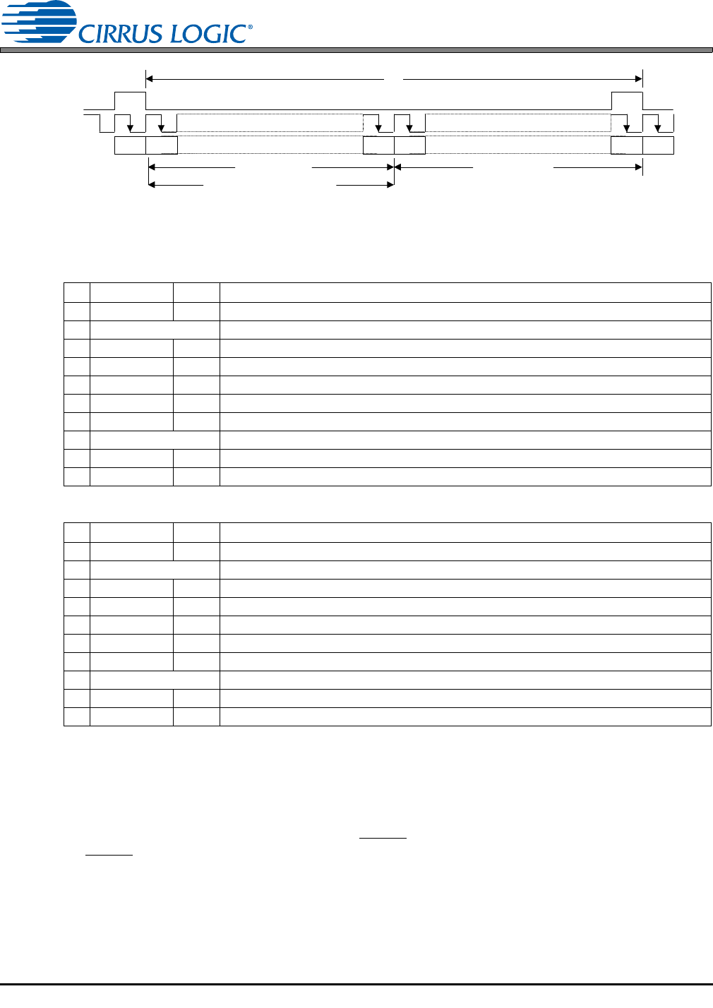
LRCK
SCLK
MSB LSB
SDIN
HP/LINE OUTB
LSB
Left Channel
Right Channel
MSB LSB MSB
Audio Word Length (AWL)
1/fs
HP/LINE OUTA
Figure 19. DSP Mode Format)