
User Manual


Table Of Contents
- 1. Pin Descriptions
- 2. Typical Connection Diagram
- 3. Characteristic and Specifications
- Recommended Operating Conditions
- Absolute Maximum Ratings
- Analog Input Characteristics
- ADC Digital Filter Characteristics
- Analog Output Characteristics
- Analog Passthrough Characteristics
- PWM Output Characteristics
- Headphone Output Power Characteristics
- Line Output Voltage Level Characteristics
- Combined DAC Interpolation and onChip Analog FIlter Response
- Switching Specifications - Serial Port
- Switching Specifications - I²C Control Port
- DC Electrical Characteristics
- Digital Interface Specifications and Characteristics
- Power Consumption
- 4. Applications
- 4.1 Overview
- 4.2 Analog Inputs
- 4.3 Analog Outputs
- 4.4 Analog In to Analog Out Passthrough
- 4.5 PWM Outputs
- 4.6 Serial Port Clocking
- 4.7 Digital Interface Formats
- 4.8 Initialization
- 4.9 Recommended Power-up Sequence
- 4.10 Recommended Power-Down Sequence
- 4.11 Required Initialization Settings
- 4.12 Control Port Operation
- 5. Register Quick Reference
- 6. Register Description
- 6.1 Chip I.D. and Revision Register (Address 01h) (Read Only)
- 6.2 Power Control 1 (Address 02h)
- 6.3 Power Control 2 (Address 03h)
- 6.4 Power Control 3 (Address 04h)
- 6.5 Clocking Control (Address 05h)
- 6.6 Interface Control 1 (Address 06h)
- 6.7 Interface Control 2 (Address 07h)
- 6.8 Input x Select: ADCA and PGAA (Address 08h), ADCB and PGAB (Address 09h)
- 6.9 Analog and HPF Control (Address 0Ah)
- 6.10 ADC HPF Corner Frequency (Address 0Bh)
- 6.11 Misc. ADC Control (Address 0Ch)
- 6.12 Playback Control 1 (Address 0Dh)
- 6.13 Miscellaneous Controls (Address 0Eh)
- 6.14 Playback Control 2 (Address 0Fh)
- 6.15 MICx Amp Control:MIC A (Address 10h) and MIC B (Address 11h)
- 6.16 PGAx Vol. and ALCx Transition Ctl.: ALC, PGA A (Address 12h) and ALC, PGA B (Address 13h)
- 6.17 Passthrough x Volume: PASSAVOL (Address 14h) and PASSBVOL (Address 15h)
- 6.18 ADCx Volume Control: ADCAVOL (Address 16h) and ADCBVOL (Address 17h)
- 6.19 ADCx Mixer Volume: ADCA (Address 18h) and ADCB (Address 19h)
- 6.20 PCMx Mixer Volume: PCMA (Address 1Ah) and PCMB (Address 1Bh)
- 6.21 Beep Frequency and On Time (Address 1Ch)
- 6.22 Beep Volume and Off Time (Address 1Dh)
- 6.23 Beep and Tone Configuration (Address 1Eh)
- 6.24 Tone Control (Address 1Fh)
- 6.25 Master Volume Control: MSTA (Address 20h) and MSTB (Address 21h)
- 6.26 Headphone Volume Control: HPA (Address 22h) and HPB (Address 23h)
- 6.27 Speaker Volume Control: SPKA (Address 24h) and SPKB (Address 25h)
- 6.28 ADC and PCM Channel Mixer (Address 26h)
- 6.29 Limiter Control 1, Min/Max Thresholds (Address 27h)
- 6.30 Limiter Control 2, Release Rate (Address 28h)
- 6.31 Limiter Attack Rate (Address 29h)
- 6.32 ALC Enable and Attack Rate (Address 2Ah)
- 6.33 ALC Release Rate (Address 2Bh)
- 6.34 ALC Threshold (Address 2Ch)
- 6.35 Noise Gate Control (Address 2Dh)
- 6.36 Status (Address 2Eh) (Read Only)
- 6.37 Battery Compensation (Address 2Fh)
- 6.38 VP Battery Level (Address 30h) (Read Only)
- 6.39 Speaker Status (Address 31h) (Read Only)
- 6.40 Charge Pump Frequency (Address 34h)
- 7. Analog Performance Plots
- 8. Example System Clock Frequencies
- 9. PCB Layout Considerations
- 10. ADC and DAC Digital Filters
- 11. Parameter Definitions
- 12. Package Dimensions
- 13. Ordering Information
- 14. References
- 15. Revision History
DS680F2 33
CS42L52
3/1/13
4.5.2 VP Battery Compensation
The CS42L52 provides the option to maintain a desired power output level, independent of the VP supply.
When enabled, this feature works by monitoring the voltage on the VP supply and reducing the attenua-
tion on the speaker outputs when VP voltage levels fall.
Note: The internal ADC that monitors the VP supply operates from the VA supply. Calculations are
based on typical VA levels of 1.8 V and 2.5 V using the VPREF bits.
4.5.2.1 Maintaining a Desired Output Level
Using SPKxVOL, the speaker output level must first be attenuated by the decibel equivalent of the expect-
ed VP supply range (MAX relative to MIN). The CS42L52 then gradually reduces the attenuation as the
VP supply drops from its maximum level, maintaining a nearly constant power output.
Compensation Example 1 (VP Battery supply ranges from 4.5 V to 3.0 V)
1. Set speaker attenuation (SPKxVOL) to -3.5 dB. The VP supply changes ~3.5 dB.
2. Set the reference VP supply (VPREF) to 4.5 V.
3. Enable battery compensation (BATTCMP).
The CS42L52 automatically adjusts the output level as the battery discharges.
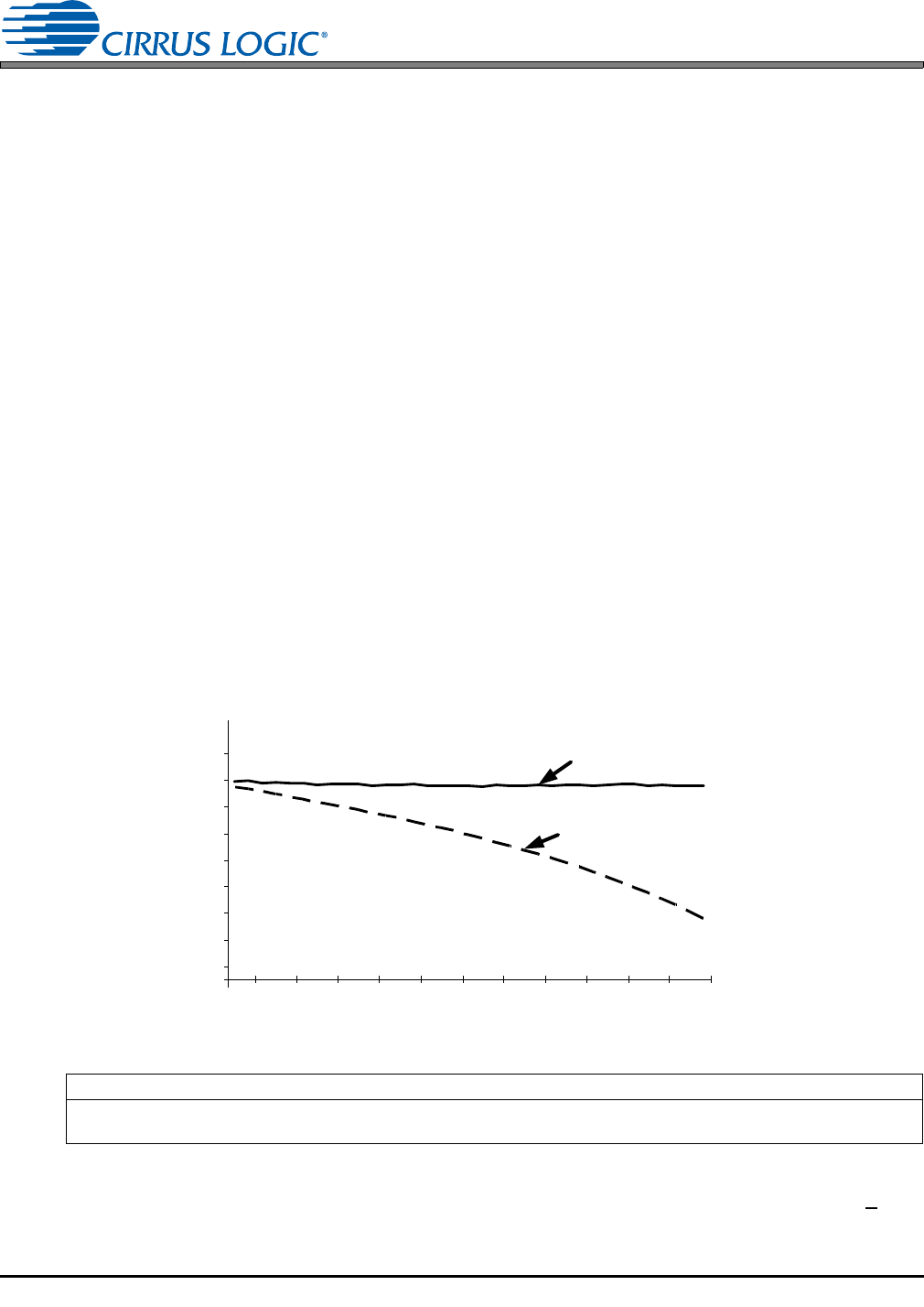
Compensation Example 2 (VP Battery supply ranges from 5.0 V to 1.6 V)
1. Set speaker attenuation (SPKxVOL) to -10 dB. The VP supply changes ~9.9 dB.
2. Set the reference VP supply (VPREF) to 5.0 V.
3. Enable battery compensation (BATTCMP).
The CS42L52 automatically adjusts the output level as the battery discharges. Refer to Figure 15 on page
33. In this example, the VP supply changes over a wide range, illustrating the accuracy of the CS42L52’s
battery compensation.
4.6 Serial Port Clocking
The CODEC serial audio interface port operates either as a slave or master, determined by the M/S bit. It
accepts externally generated clocks in Slave Mode and will generate synchronous clocks derived from an
Referenced Control Register Location
VPREF ................................
SPKxVOL ............................
“VP Reference” on page 72
“Speaker Volume Control” on page 64
-24
-22
-20
-18
-16
-14
-12
-10
-8
-6
1.61.92.22.52.83.13.43.744.34.64.9
Uncompensated
PWM Output
Level
Battery Compensated
PWM Output Level
VP Supply (V)
PWM Output Level (dB)
Figure 15. Battery Compensation