
User Manual


Table Of Contents
- 1. Pin Descriptions
- 2. Typical Connection Diagram
- 3. Characteristic and Specifications
- Recommended Operating Conditions
- Absolute Maximum Ratings
- Analog Input Characteristics
- ADC Digital Filter Characteristics
- Analog Output Characteristics
- Analog Passthrough Characteristics
- PWM Output Characteristics
- Headphone Output Power Characteristics
- Line Output Voltage Level Characteristics
- Combined DAC Interpolation and onChip Analog FIlter Response
- Switching Specifications - Serial Port
- Switching Specifications - I²C Control Port
- DC Electrical Characteristics
- Digital Interface Specifications and Characteristics
- Power Consumption
- 4. Applications
- 4.1 Overview
- 4.2 Analog Inputs
- 4.3 Analog Outputs
- 4.4 Analog In to Analog Out Passthrough
- 4.5 PWM Outputs
- 4.6 Serial Port Clocking
- 4.7 Digital Interface Formats
- 4.8 Initialization
- 4.9 Recommended Power-up Sequence
- 4.10 Recommended Power-Down Sequence
- 4.11 Required Initialization Settings
- 4.12 Control Port Operation
- 5. Register Quick Reference
- 6. Register Description
- 6.1 Chip I.D. and Revision Register (Address 01h) (Read Only)
- 6.2 Power Control 1 (Address 02h)
- 6.3 Power Control 2 (Address 03h)
- 6.4 Power Control 3 (Address 04h)
- 6.5 Clocking Control (Address 05h)
- 6.6 Interface Control 1 (Address 06h)
- 6.7 Interface Control 2 (Address 07h)
- 6.8 Input x Select: ADCA and PGAA (Address 08h), ADCB and PGAB (Address 09h)
- 6.9 Analog and HPF Control (Address 0Ah)
- 6.10 ADC HPF Corner Frequency (Address 0Bh)
- 6.11 Misc. ADC Control (Address 0Ch)
- 6.12 Playback Control 1 (Address 0Dh)
- 6.13 Miscellaneous Controls (Address 0Eh)
- 6.14 Playback Control 2 (Address 0Fh)
- 6.15 MICx Amp Control:MIC A (Address 10h) and MIC B (Address 11h)
- 6.16 PGAx Vol. and ALCx Transition Ctl.: ALC, PGA A (Address 12h) and ALC, PGA B (Address 13h)
- 6.17 Passthrough x Volume: PASSAVOL (Address 14h) and PASSBVOL (Address 15h)
- 6.18 ADCx Volume Control: ADCAVOL (Address 16h) and ADCBVOL (Address 17h)
- 6.19 ADCx Mixer Volume: ADCA (Address 18h) and ADCB (Address 19h)
- 6.20 PCMx Mixer Volume: PCMA (Address 1Ah) and PCMB (Address 1Bh)
- 6.21 Beep Frequency and On Time (Address 1Ch)
- 6.22 Beep Volume and Off Time (Address 1Dh)
- 6.23 Beep and Tone Configuration (Address 1Eh)
- 6.24 Tone Control (Address 1Fh)
- 6.25 Master Volume Control: MSTA (Address 20h) and MSTB (Address 21h)
- 6.26 Headphone Volume Control: HPA (Address 22h) and HPB (Address 23h)
- 6.27 Speaker Volume Control: SPKA (Address 24h) and SPKB (Address 25h)
- 6.28 ADC and PCM Channel Mixer (Address 26h)
- 6.29 Limiter Control 1, Min/Max Thresholds (Address 27h)
- 6.30 Limiter Control 2, Release Rate (Address 28h)
- 6.31 Limiter Attack Rate (Address 29h)
- 6.32 ALC Enable and Attack Rate (Address 2Ah)
- 6.33 ALC Release Rate (Address 2Bh)
- 6.34 ALC Threshold (Address 2Ch)
- 6.35 Noise Gate Control (Address 2Dh)
- 6.36 Status (Address 2Eh) (Read Only)
- 6.37 Battery Compensation (Address 2Fh)
- 6.38 VP Battery Level (Address 30h) (Read Only)
- 6.39 Speaker Status (Address 31h) (Read Only)
- 6.40 Charge Pump Frequency (Address 34h)
- 7. Analog Performance Plots
- 8. Example System Clock Frequencies
- 9. PCB Layout Considerations
- 10. ADC and DAC Digital Filters
- 11. Parameter Definitions
- 12. Package Dimensions
- 13. Ordering Information
- 14. References
- 15. Revision History
DS680F2 29
CS42L52
3/1/13
4.3.1 Beep Generator
The Beep Generator generates audio frequencies across approximately two octave major scales. It offers
three modes of operation: Continuous, multiple, and single (one-shot) beeps. Sixteen on and eight off
times are available.
Note: The Beep is generated before the limiter and may affect desired limiting performance. If the lim-
iter function is used, it may be required to set the beep volume sufficiently below the threshold to prevent
the peak detect from triggering. Since the master volume control, MSTxVOL[7:0], will affect the beep vol-
ume, DAC volume may alternatively be controlled using the PMIXxVOL[6:0] bits.
Referenced Control Register Location
PWM Control
SPKxMUTE .........................
MUTE50/50 .........................
SPKMONO..........................
SPKxVOL[7:0] .....................
SPKSWAP...........................
SPKB=A ..............................
BATTCMP ...........................
VPREF[3:0] .........................
VPLVL[7:0] ..........................
PDN_SPKx[1:0]...................
SPKxSHRT..........................
“Speaker Mute” on page 54
“Speaker Mute 50/50 Control” on page 54
“Speaker MONO Control” on page 54
“Speaker Volume Control” on page 64
“Speaker Channel Swap” on page 54
“Speaker Volume Setting B=A” on page 54
“Battery Compensation” on page 71
“VP Reference” on page 72
“VP Voltage Level (Read Only)” on page 72
“Speaker Power Control” on page 44
“Speaker Current Load Status (Read Only)” on page 72
Referenced Control Register Location
Analog Output
HPxMUTE ...........................
HPxVOL[7:0] .......................
PDN_HPx[1:0].....................
HPGAIN[2:0]........................
PASSTHRUx .......................
PASSxMUTE .......................
PASSxVOL[7:0] ...................
CHGFREQ ..........................
“Headphone Mute” on page 54
“Headphone Volume Control” on page 63
“Headphone Power Control” on page 44
“Headphone Analog Gain” on page 51
“Passthrough Analog” on page 52
“Passthrough Mute” on page 52
“Passthrough x Volume” on page 57
“Charge Pump Frequency” on page 73
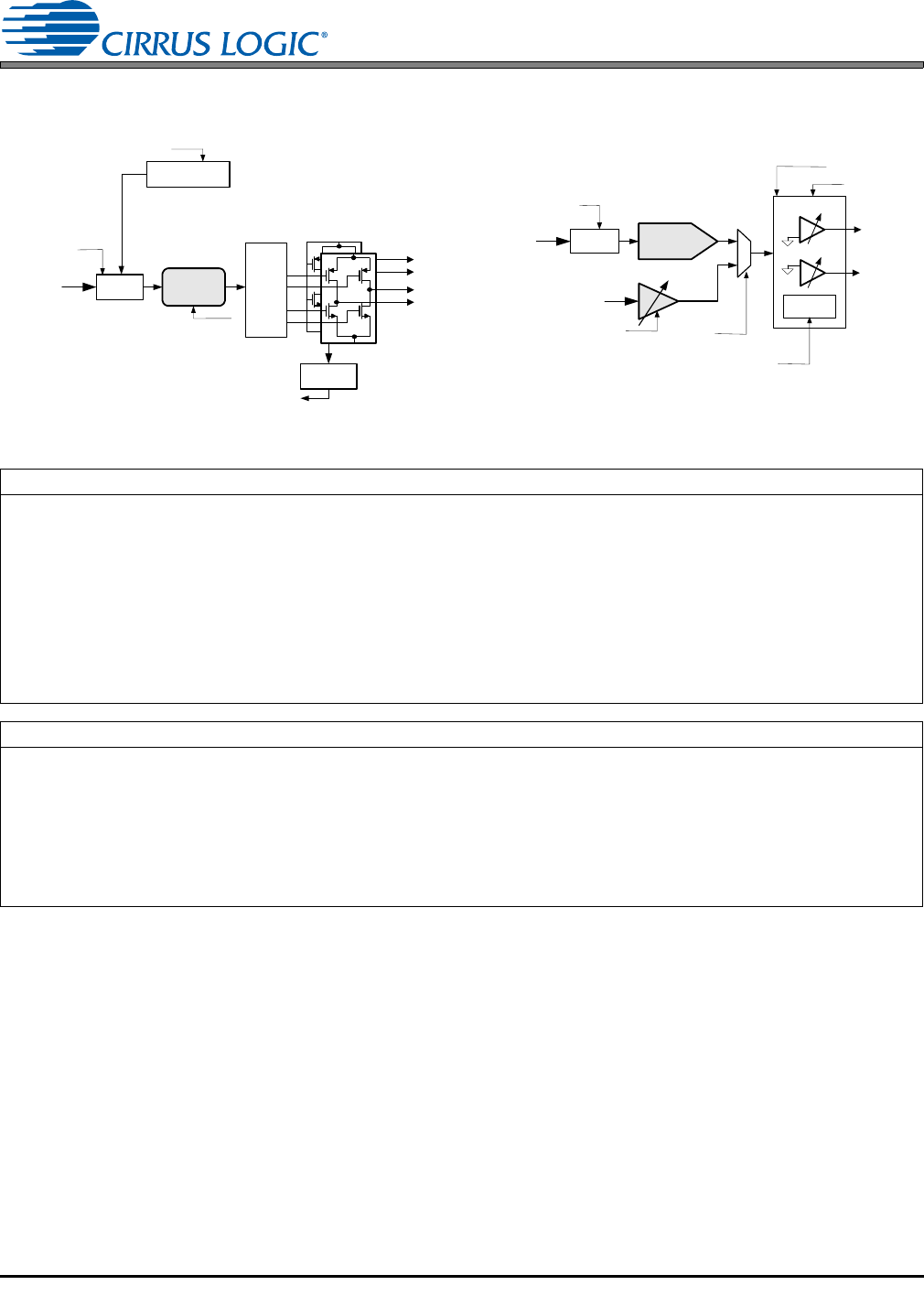
Charge
Pump
DAC
CHGFREQ[3:0]
HPGAIN[2:0]
VOL
VOL
Analog Passthru
from PGA
HPAMUTE
HPBMUTE
HPA_VOL[7:0]
HPB_VOL[7:0]
+0dB/-102dB
0.5dB steps
PASSAMUTE
PASSBMUTE
PASSAVOL[7:0]
PASSBVOL[70]
+12dB/-60dB
0.5dB steps
(uses PGA)
PASSTHRUA
PASSTHRUB
PDN_HPA[1:0]
PDN_HPB[1:0]
A
B
from DSP
Engine
HP/Line
Outputs
VOL
PWM
Modulator
A
SPKAMUTE
SPKBMUTE
MUTE50/50
SPKMONO
SPKSWAP
SPKB=A
SPKAVOL[7:0]
SPKBVOL[7:0]
+0dB/-102dB
0.5dB steps
PDN_SPKA[1:0]
PDN_SPKB[1:0]
Short
Circuit
SPKASHRT
Battery
Compensation
BATTCMP
VPREF[3:0]
VPLVL[7:0]
SPKBSHRT
+
-
+
-
Gate
Drive
from DSP
Engine
Speaker
Outputs
B
Figure 11. PWM Output Stage Figure 12. Analog Output Stage