
User Manual


Table Of Contents
- 1. Pin Descriptions
- 2. Typical Connection Diagram
- 3. Characteristic and Specifications
- Recommended Operating Conditions
- Absolute Maximum Ratings
- Analog Input Characteristics
- ADC Digital Filter Characteristics
- Analog Output Characteristics
- Analog Passthrough Characteristics
- PWM Output Characteristics
- Headphone Output Power Characteristics
- Line Output Voltage Level Characteristics
- Combined DAC Interpolation and onChip Analog FIlter Response
- Switching Specifications - Serial Port
- Switching Specifications - I²C Control Port
- DC Electrical Characteristics
- Digital Interface Specifications and Characteristics
- Power Consumption
- 4. Applications
- 4.1 Overview
- 4.2 Analog Inputs
- 4.3 Analog Outputs
- 4.4 Analog In to Analog Out Passthrough
- 4.5 PWM Outputs
- 4.6 Serial Port Clocking
- 4.7 Digital Interface Formats
- 4.8 Initialization
- 4.9 Recommended Power-up Sequence
- 4.10 Recommended Power-Down Sequence
- 4.11 Required Initialization Settings
- 4.12 Control Port Operation
- 5. Register Quick Reference
- 6. Register Description
- 6.1 Chip I.D. and Revision Register (Address 01h) (Read Only)
- 6.2 Power Control 1 (Address 02h)
- 6.3 Power Control 2 (Address 03h)
- 6.4 Power Control 3 (Address 04h)
- 6.5 Clocking Control (Address 05h)
- 6.6 Interface Control 1 (Address 06h)
- 6.7 Interface Control 2 (Address 07h)
- 6.8 Input x Select: ADCA and PGAA (Address 08h), ADCB and PGAB (Address 09h)
- 6.9 Analog and HPF Control (Address 0Ah)
- 6.10 ADC HPF Corner Frequency (Address 0Bh)
- 6.11 Misc. ADC Control (Address 0Ch)
- 6.12 Playback Control 1 (Address 0Dh)
- 6.13 Miscellaneous Controls (Address 0Eh)
- 6.14 Playback Control 2 (Address 0Fh)
- 6.15 MICx Amp Control:MIC A (Address 10h) and MIC B (Address 11h)
- 6.16 PGAx Vol. and ALCx Transition Ctl.: ALC, PGA A (Address 12h) and ALC, PGA B (Address 13h)
- 6.17 Passthrough x Volume: PASSAVOL (Address 14h) and PASSBVOL (Address 15h)
- 6.18 ADCx Volume Control: ADCAVOL (Address 16h) and ADCBVOL (Address 17h)
- 6.19 ADCx Mixer Volume: ADCA (Address 18h) and ADCB (Address 19h)
- 6.20 PCMx Mixer Volume: PCMA (Address 1Ah) and PCMB (Address 1Bh)
- 6.21 Beep Frequency and On Time (Address 1Ch)
- 6.22 Beep Volume and Off Time (Address 1Dh)
- 6.23 Beep and Tone Configuration (Address 1Eh)
- 6.24 Tone Control (Address 1Fh)
- 6.25 Master Volume Control: MSTA (Address 20h) and MSTB (Address 21h)
- 6.26 Headphone Volume Control: HPA (Address 22h) and HPB (Address 23h)
- 6.27 Speaker Volume Control: SPKA (Address 24h) and SPKB (Address 25h)
- 6.28 ADC and PCM Channel Mixer (Address 26h)
- 6.29 Limiter Control 1, Min/Max Thresholds (Address 27h)
- 6.30 Limiter Control 2, Release Rate (Address 28h)
- 6.31 Limiter Attack Rate (Address 29h)
- 6.32 ALC Enable and Attack Rate (Address 2Ah)
- 6.33 ALC Release Rate (Address 2Bh)
- 6.34 ALC Threshold (Address 2Ch)
- 6.35 Noise Gate Control (Address 2Dh)
- 6.36 Status (Address 2Eh) (Read Only)
- 6.37 Battery Compensation (Address 2Fh)
- 6.38 VP Battery Level (Address 30h) (Read Only)
- 6.39 Speaker Status (Address 31h) (Read Only)
- 6.40 Charge Pump Frequency (Address 34h)
- 7. Analog Performance Plots
- 8. Example System Clock Frequencies
- 9. PCB Layout Considerations
- 10. ADC and DAC Digital Filters
- 11. Parameter Definitions
- 12. Package Dimensions
- 13. Ordering Information
- 14. References
- 15. Revision History
26 DS680F2
CS42L52
3/1/13
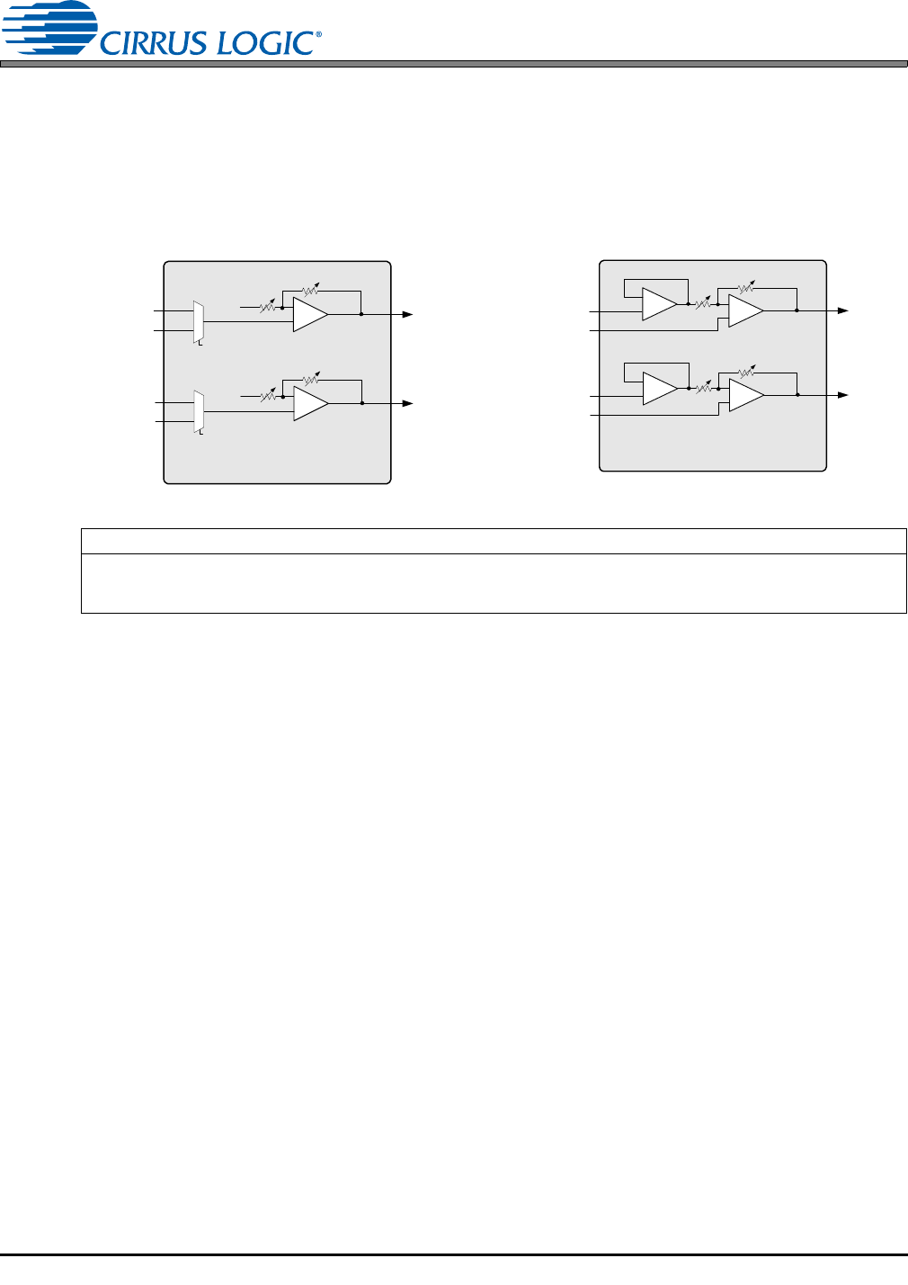
4.2.1 MIC Inputs
The input pins 21, 22, 23, and 24 accept stereo line-level or microphone signals. For microphone inputs,
either single-ended or differential configuration is allowed, providing programmable pre-amplification of
low-level signals. In the single-ended configuration, an internal MUX chooses one of two stereo sets (se-
lection is made independently on channels A and B). In the differential configuration, an internal voltage
follower cascaded with the pre-amplifier maintains high input impedance and provides noise rejection
above the MICxGAIN setting. The pre-amps are biased to VQ in both configurations.
4.2.2 Automatic Level Control (ALC)
When enabled, the ALC monitors the analog input signal after the digital attenuator, detects when peak
levels exceed the maximum (MAX) threshold settings, and responds by applying attenuation as neces-
sary to maintain the resulting level below the MAX threshold. To apply this attenuation, the ALC first low-
ers the PGA gain settings and then increases the digital attenuation levels. All attenuation is applied at a
programmable attack rate.
When input signal levels fall below the minimum (MIN) threshold, the ALC responds by removing any at-
tenuation that it has previously applied until all ALC-applied attenuation has been removed or until the
MAX threshold is again crossed. To remove this attenuation, the ALC first decreases the digital attenua-
tion levels and then increases the PGA gain. All attenuation is removed at a programmable release rate.
It should be noted that the ALC is applied independently to channels A and B with one exception: the input
signals on both channels A and B must be below the MIN threshold in order for the ALC attenuation to be
released on channel B.
Attack and release rates are affected by the ADC soft-ramp/zero-cross settings and sample rate, Fs. ALC
soft-ramp and zero-cross dependency may be independently enabled/disabled.
Recommended settings: Best level control may be realized with the fastest attack and slowest release
setting with soft ramp enabled in the control registers.
Notes:
1. When ALC x is enabled and the PGAxVOL[5:0] is set above 12 dB, the ADCxVOL[7:0] should not be
set below 0 dB.
2. The maximum realized gain must be set in the PGAxVOL register. The ALC will only apply the gain
set in the PGAxVOL.
3. The ALC maintains the output signal between the MIN/MAX thresholds. As input signal level changes,
the level-controlled output may not always be the same but always falls within the thresholds.
Referenced Control Register Location
MICxCFG ............................
PDN_MICx ..........................
MICxGAIN...........................
“MICx Configuration” on page 55
“Power Down MICx” on page 43
“MICx Gain” on page 55
MIC1-
-
+
-
+
MIC1+
MIC2-
-
+
-
+
MIC2+
23
21
24
22
MICACFG=’1'b
MICBCFG=’1'b
MICAGAIN[4:0]
MICBGAIN[4:0]
16..32 dB/
1 dB steps
16..32 dB/
1 dB steps
PDN_MICA=’0'b
PDN_MICB=’0'b
to summing
PGA A
Note: Output to PGA = (MIC
+
- MIC
-
)*gain + MIC
-
to summing
PGA B
MIC1A
-
+
MIC2A
MIC1B
-
+
MIC2B
23
21
24
22
MICACFG=’0'b
MICBCFG=’0'b
MICAGAIN[4:0]
MICBGAIN[4:0]
16..32 dB/
1 dB steps
16..32 dB/
1 dB steps
PDN_MICA=’0'b
PDN_MICB=’0'b
MICASEL
MICBSEL
to summing
PGA A
to summing
PGA B
VQ
VQ
Figure 6. Single-Ended MIC Configuration Figure 7. Differential MIC Configuration