
User Manual


Table Of Contents
- 1. Pin Descriptions
- 2. Typical Connection Diagram
- 3. Characteristic and Specifications
- Recommended Operating Conditions
- Absolute Maximum Ratings
- Analog Input Characteristics
- ADC Digital Filter Characteristics
- Analog Output Characteristics
- Analog Passthrough Characteristics
- PWM Output Characteristics
- Headphone Output Power Characteristics
- Line Output Voltage Level Characteristics
- Combined DAC Interpolation and onChip Analog FIlter Response
- Switching Specifications - Serial Port
- Switching Specifications - I²C Control Port
- DC Electrical Characteristics
- Digital Interface Specifications and Characteristics
- Power Consumption
- 4. Applications
- 4.1 Overview
- 4.2 Analog Inputs
- 4.3 Analog Outputs
- 4.4 Analog In to Analog Out Passthrough
- 4.5 PWM Outputs
- 4.6 Serial Port Clocking
- 4.7 Digital Interface Formats
- 4.8 Initialization
- 4.9 Recommended Power-up Sequence
- 4.10 Recommended Power-Down Sequence
- 4.11 Required Initialization Settings
- 4.12 Control Port Operation
- 5. Register Quick Reference
- 6. Register Description
- 6.1 Chip I.D. and Revision Register (Address 01h) (Read Only)
- 6.2 Power Control 1 (Address 02h)
- 6.3 Power Control 2 (Address 03h)
- 6.4 Power Control 3 (Address 04h)
- 6.5 Clocking Control (Address 05h)
- 6.6 Interface Control 1 (Address 06h)
- 6.7 Interface Control 2 (Address 07h)
- 6.8 Input x Select: ADCA and PGAA (Address 08h), ADCB and PGAB (Address 09h)
- 6.9 Analog and HPF Control (Address 0Ah)
- 6.10 ADC HPF Corner Frequency (Address 0Bh)
- 6.11 Misc. ADC Control (Address 0Ch)
- 6.12 Playback Control 1 (Address 0Dh)
- 6.13 Miscellaneous Controls (Address 0Eh)
- 6.14 Playback Control 2 (Address 0Fh)
- 6.15 MICx Amp Control:MIC A (Address 10h) and MIC B (Address 11h)
- 6.16 PGAx Vol. and ALCx Transition Ctl.: ALC, PGA A (Address 12h) and ALC, PGA B (Address 13h)
- 6.17 Passthrough x Volume: PASSAVOL (Address 14h) and PASSBVOL (Address 15h)
- 6.18 ADCx Volume Control: ADCAVOL (Address 16h) and ADCBVOL (Address 17h)
- 6.19 ADCx Mixer Volume: ADCA (Address 18h) and ADCB (Address 19h)
- 6.20 PCMx Mixer Volume: PCMA (Address 1Ah) and PCMB (Address 1Bh)
- 6.21 Beep Frequency and On Time (Address 1Ch)
- 6.22 Beep Volume and Off Time (Address 1Dh)
- 6.23 Beep and Tone Configuration (Address 1Eh)
- 6.24 Tone Control (Address 1Fh)
- 6.25 Master Volume Control: MSTA (Address 20h) and MSTB (Address 21h)
- 6.26 Headphone Volume Control: HPA (Address 22h) and HPB (Address 23h)
- 6.27 Speaker Volume Control: SPKA (Address 24h) and SPKB (Address 25h)
- 6.28 ADC and PCM Channel Mixer (Address 26h)
- 6.29 Limiter Control 1, Min/Max Thresholds (Address 27h)
- 6.30 Limiter Control 2, Release Rate (Address 28h)
- 6.31 Limiter Attack Rate (Address 29h)
- 6.32 ALC Enable and Attack Rate (Address 2Ah)
- 6.33 ALC Release Rate (Address 2Bh)
- 6.34 ALC Threshold (Address 2Ch)
- 6.35 Noise Gate Control (Address 2Dh)
- 6.36 Status (Address 2Eh) (Read Only)
- 6.37 Battery Compensation (Address 2Fh)
- 6.38 VP Battery Level (Address 30h) (Read Only)
- 6.39 Speaker Status (Address 31h) (Read Only)
- 6.40 Charge Pump Frequency (Address 34h)
- 7. Analog Performance Plots
- 8. Example System Clock Frequencies
- 9. PCB Layout Considerations
- 10. ADC and DAC Digital Filters
- 11. Parameter Definitions
- 12. Package Dimensions
- 13. Ordering Information
- 14. References
- 15. Revision History
DS680F2 25
CS42L52
3/1/13
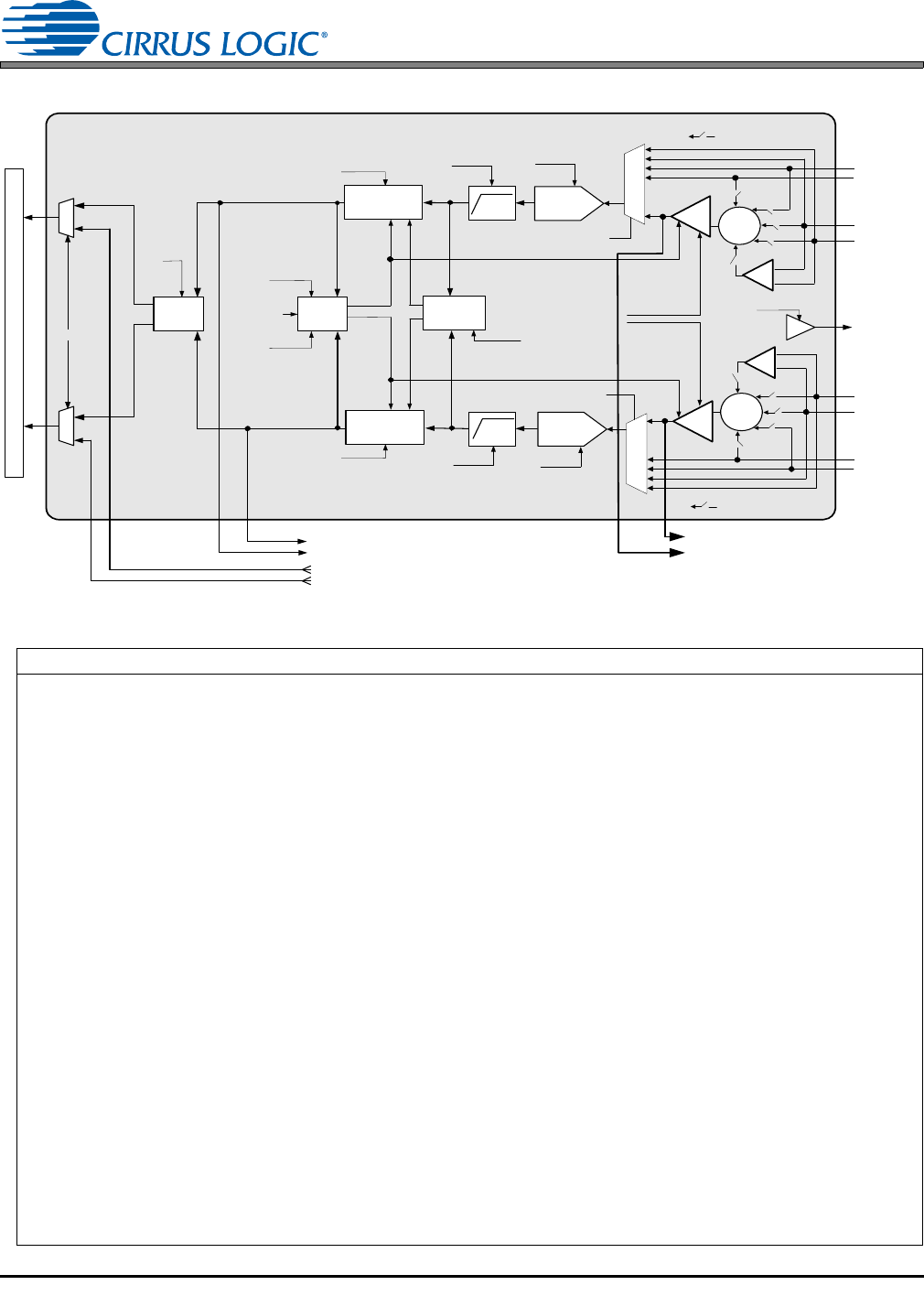
4.2 Analog Inputs
Referenced Control Register Location
Analog Front End
PDN_PGAx .........................
PGAxVOL[5:0].....................
ADCB=A..............................
ANLGSFTx..........................
ANLGZCx............................
ADCxSEL[2:0] .....................
PGAxSEL5,4,3,2,1 ..............
BIASLVL[2:0] .......................
PDN_BIAS...........................
PDN_ADCx .........................
PDN_CHRG ........................
INV_ADCx...........................
HPFRZx...............................
HPFx ...................................
HPFx_CF[1:0]......................
ADCxOVFL..........................
Digital Volume
ADCxMUTE.........................
ADCxVOL............................
ALCx....................................
ALCxSRDIS.........................
ALCxZCDIS.........................
ALCARATE[5:0]...................
ALCRRATE[5:0] ..................
MAX[2:0]..............................
MIN[2:0]...............................
NGALL.................................
NG.......................................
THRESH[3:0].......................
NGDELAY[1:0] ....................
Miscellaneous
DIGSUM[1:0].......................
DIGMUX..............................
“Power Down PGAx” on page 42
“PGAx Volume” on page 56
“Analog Front-End Volume Setting B=A” on page 50
“Ch. x Analog Soft Ramp” on page 49
“Ch. x Analog Zero Cross” on page 49
“ADC Input Select” on page 48
“PGA Input Mapping” on page 49
“MIC Bias Level” on page 48
“Power Down MIC Bias” on page 43
“Power Down ADCx” on page 43
“Power Down ADC Charge Pump” on page 42
“Invert ADC Signal Polarity” on page 51
“ADCx High-Pass Filter Freeze” on page 49
“ADCx High-Pass Filter” on page 49
“HPF x Corner Frequency” on page 50
“ADCx Overflow (Read Only)” on page 71
“ADC Mute” on page 51
“ADCx Volume” on page 57
“ALCx Enable” on page 67
“ALCx Soft Ramp Disable” on page 55
“ALCx Zero Cross Disable” on page 56
“ALC Attack Rate” on page 67
“ALC Release Rate” on page 68
“ALC Maximum Threshold” on page 68
“ALC Minimum Threshold” on page 69
“Noise Gate All Channels” on page 69
“Noise Gate Enable” on page 69
“Noise Gate Threshold and Boost” on page 70
“Noise Gate Delay Timing” on page 70
“Digital Sum” on page 50
“Digital MUX” on page 50
`
AIN4A/ MIC1+/
MIC2A
Gain Adjust
ALC
PDN_PGAA
PGAAVOL[5:0]
ADCB=A
ANLGSFTA
ANLGZCA
HPFRZA
HPFA
HPFA_CF[1:0]
PDN_ADCA
INV_ADCA
PDN_CHRG
ALCB
ALCBSRDIS
ALCBZCDIS
MICBIAS
BIASLVL[2:0]
PDN_BIAS
PCM Serial Interface
TO DSP Engine
ALCARATE[5:0]
ALCRRATE[5:0]
MAX[2:0]
MIN[2:0]
ALCA
ALCASRDIS
ALCAZCDIS
AIN1A
AIN2A
= PGAASEL[5:1]
ADC
PDN_PGAB
PGABVOL[5:0]
ADCB=A
ANLGSFTB
ANLGZCB
ADCBMUTE
DIGSFT
DIGZC
ADCBVOL[7:0]
+24/-96dB
1dB steps
HPFRZB
HPB
HPFB_CF[1:0]
PDN_ADCB
INV_ADCB
PDN_CHRG
Noise Gate
NGALL
NG
THRESH[3:0]
NGDELAY[1:0]
Gain Adjust
FROM DSP ENGINE
DIGMIX
AIN3A/MIC1-/
MIC1A
AIN4B/ MIC2+/
MIC2B
AIN1B
AIN2B
AIN3B/MIC2-/
MIC1B
ANALOG PASS THRU TO
HEADPHONE AMPLIFIER MUX
Swap/
Mix
DIGSUM[1:0]
ADCAMUTE
DIGSFT
DIGZC
ADCAVOL[7:0]
+24/-96dB
1dB steps
Refer to
“MIC Inputs”
ADC
ADCASEL[2:0]
ADCBSEL[2:0]
= PGABSEL[5:1]
Refer to
“MIC Inputs”
Figure 5. Analog Input Signal Flow