
User Manual


Table Of Contents
- 1. Pin Descriptions
- 2. Typical Connection Diagram
- 3. Characteristic and Specifications
- Recommended Operating Conditions
- Absolute Maximum Ratings
- Analog Input Characteristics
- ADC Digital Filter Characteristics
- Analog Output Characteristics
- Analog Passthrough Characteristics
- PWM Output Characteristics
- Headphone Output Power Characteristics
- Line Output Voltage Level Characteristics
- Combined DAC Interpolation and onChip Analog FIlter Response
- Switching Specifications - Serial Port
- Switching Specifications - I²C Control Port
- DC Electrical Characteristics
- Digital Interface Specifications and Characteristics
- Power Consumption
- 4. Applications
- 4.1 Overview
- 4.2 Analog Inputs
- 4.3 Analog Outputs
- 4.4 Analog In to Analog Out Passthrough
- 4.5 PWM Outputs
- 4.6 Serial Port Clocking
- 4.7 Digital Interface Formats
- 4.8 Initialization
- 4.9 Recommended Power-up Sequence
- 4.10 Recommended Power-Down Sequence
- 4.11 Required Initialization Settings
- 4.12 Control Port Operation
- 5. Register Quick Reference
- 6. Register Description
- 6.1 Chip I.D. and Revision Register (Address 01h) (Read Only)
- 6.2 Power Control 1 (Address 02h)
- 6.3 Power Control 2 (Address 03h)
- 6.4 Power Control 3 (Address 04h)
- 6.5 Clocking Control (Address 05h)
- 6.6 Interface Control 1 (Address 06h)
- 6.7 Interface Control 2 (Address 07h)
- 6.8 Input x Select: ADCA and PGAA (Address 08h), ADCB and PGAB (Address 09h)
- 6.9 Analog and HPF Control (Address 0Ah)
- 6.10 ADC HPF Corner Frequency (Address 0Bh)
- 6.11 Misc. ADC Control (Address 0Ch)
- 6.12 Playback Control 1 (Address 0Dh)
- 6.13 Miscellaneous Controls (Address 0Eh)
- 6.14 Playback Control 2 (Address 0Fh)
- 6.15 MICx Amp Control:MIC A (Address 10h) and MIC B (Address 11h)
- 6.16 PGAx Vol. and ALCx Transition Ctl.: ALC, PGA A (Address 12h) and ALC, PGA B (Address 13h)
- 6.17 Passthrough x Volume: PASSAVOL (Address 14h) and PASSBVOL (Address 15h)
- 6.18 ADCx Volume Control: ADCAVOL (Address 16h) and ADCBVOL (Address 17h)
- 6.19 ADCx Mixer Volume: ADCA (Address 18h) and ADCB (Address 19h)
- 6.20 PCMx Mixer Volume: PCMA (Address 1Ah) and PCMB (Address 1Bh)
- 6.21 Beep Frequency and On Time (Address 1Ch)
- 6.22 Beep Volume and Off Time (Address 1Dh)
- 6.23 Beep and Tone Configuration (Address 1Eh)
- 6.24 Tone Control (Address 1Fh)
- 6.25 Master Volume Control: MSTA (Address 20h) and MSTB (Address 21h)
- 6.26 Headphone Volume Control: HPA (Address 22h) and HPB (Address 23h)
- 6.27 Speaker Volume Control: SPKA (Address 24h) and SPKB (Address 25h)
- 6.28 ADC and PCM Channel Mixer (Address 26h)
- 6.29 Limiter Control 1, Min/Max Thresholds (Address 27h)
- 6.30 Limiter Control 2, Release Rate (Address 28h)
- 6.31 Limiter Attack Rate (Address 29h)
- 6.32 ALC Enable and Attack Rate (Address 2Ah)
- 6.33 ALC Release Rate (Address 2Bh)
- 6.34 ALC Threshold (Address 2Ch)
- 6.35 Noise Gate Control (Address 2Dh)
- 6.36 Status (Address 2Eh) (Read Only)
- 6.37 Battery Compensation (Address 2Fh)
- 6.38 VP Battery Level (Address 30h) (Read Only)
- 6.39 Speaker Status (Address 31h) (Read Only)
- 6.40 Charge Pump Frequency (Address 34h)
- 7. Analog Performance Plots
- 8. Example System Clock Frequencies
- 9. PCB Layout Considerations
- 10. ADC and DAC Digital Filters
- 11. Parameter Definitions
- 12. Package Dimensions
- 13. Ordering Information
- 14. References
- 15. Revision History
DS680F2 19
CS42L52
3/1/13
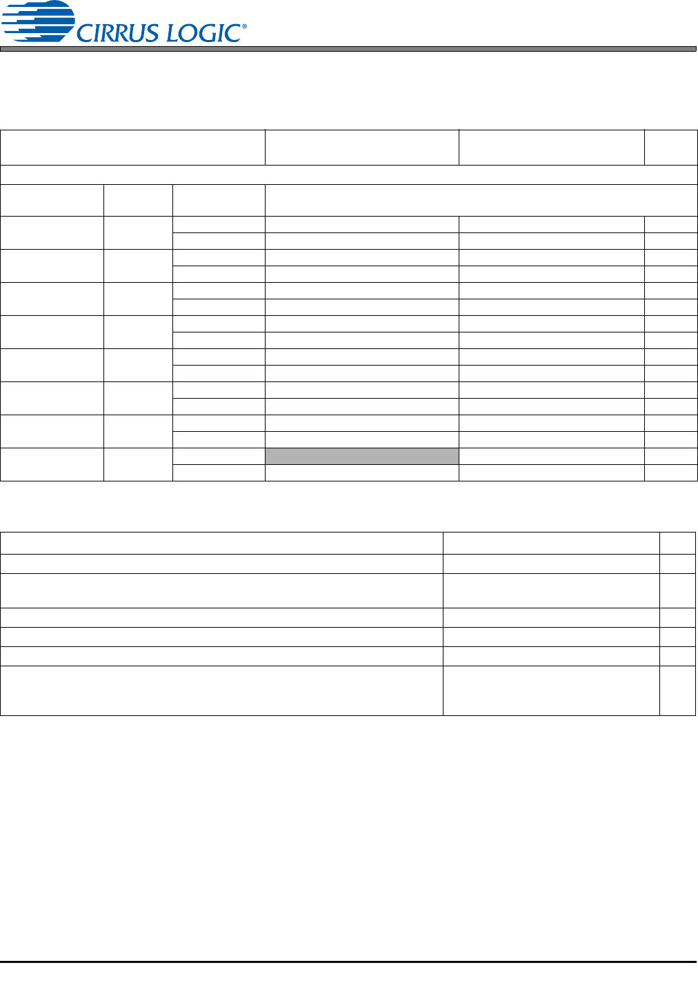
LINE OUTPUT VOLTAGE LEVEL CHARACTERISTICS
Test conditions (unless otherwise specified): Input test signal is a full-scale 997 Hz sine wave; measurement bandwidth is 20 Hz
to 20 kHz; Sample Frequency = 48 kHz; Test load R
L
= 10 k C
L
= 10 pF (see Figure 2); “Required Initialization Settings” on
page 37 written on power up.
COMBINED DAC INTERPOLATION AND ONCHIP ANALOG FILTER RESPONSE
12. Response is clock dependent and scales with Fs. Note that the response plots (Figures 30 and 33 on
page 78) have been normalized to Fs and can be de-normalized by multiplying the X-axis scale by Fs.
13. Measurement Bandwidth is from Stopband to 3 Fs.
Parameters VA = 2.5V
Min Typ Max
VA = 1.8V
Min Typ Max
Unit
AOUTx Voltage Into R
L
= 10 k
HP_GAIN[2:0] Analog
Gain (G)
VHP
000 0.3959 1.8 V - 1.34 - - 0.97 - V
pp
2.5 V - 1.34 - - 0.97 - V
pp
001 0.4571 1.8 V - 1.55 - - 1.12 - V
pp
2.5 V - 1.55 - - 1.12 - V
pp
010 0.5111 1.8 V - 1.73 - - 1.25 - V
pp
2.5 V - 1.73 - - 1.25 - V
pp
011 (default) 0.6047 1.8 V - 2.05 - 1.41 1.48 1.55 V
pp
2.5 V 1.95 2.05 2.15 - 1.48 - V
pp
100 0.7099 1.8 V - 2.41 - - 1.73 - V
pp
2.5 V - 2.41 - - 1.73 - V
pp
101 0.8399 1.8 V - 2.85 - 2.05 V
pp
2.5 V - 2.85 - - 2.05 - V
pp
110 1.0000 1.8 V - 3.39 - - 2.44 - V
pp
2.5 V - 3.39 - - 2.44 - V
pp
111 1.1430 1.8 V (See (Note 11) -2.79-V
pp
2.5 V - 3.88 - - 2.79 - V
pp
Parameters (Note 12) Min Typ Max Unit
Frequency Response 10 Hz to 20 kHz -0.01 - +0.08 dB
Passband to -0.05 dB corner
to -3 dB corner
0
0
-
-
0.4780
0.4996
Fs
Fs
StopBand 0.5465 - - Fs
StopBand Attenuation (Note 13) 50 - - dB
Group Delay - 9/Fs - s
De-emphasis Error Fs = 32 kHz
Fs = 44.1 kHz
Fs = 48 kHz
-
-
-
-
-
-
+1.5/+0
+0.05/-0.25
-0.2/-0.4
dB
dB
dB