
User Manual

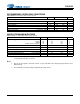


Table Of Contents
- 1. Pin Descriptions
- 2. Typical Connection Diagram
- 3. Characteristic and Specifications
- Recommended Operating Conditions
- Absolute Maximum Ratings
- Analog Input Characteristics
- ADC Digital Filter Characteristics
- Analog Output Characteristics
- Analog Passthrough Characteristics
- PWM Output Characteristics
- Headphone Output Power Characteristics
- Line Output Voltage Level Characteristics
- Combined DAC Interpolation and onChip Analog FIlter Response
- Switching Specifications - Serial Port
- Switching Specifications - I²C Control Port
- DC Electrical Characteristics
- Digital Interface Specifications and Characteristics
- Power Consumption
- 4. Applications
- 4.1 Overview
- 4.2 Analog Inputs
- 4.3 Analog Outputs
- 4.4 Analog In to Analog Out Passthrough
- 4.5 PWM Outputs
- 4.6 Serial Port Clocking
- 4.7 Digital Interface Formats
- 4.8 Initialization
- 4.9 Recommended Power-up Sequence
- 4.10 Recommended Power-Down Sequence
- 4.11 Required Initialization Settings
- 4.12 Control Port Operation
- 5. Register Quick Reference
- 6. Register Description
- 6.1 Chip I.D. and Revision Register (Address 01h) (Read Only)
- 6.2 Power Control 1 (Address 02h)
- 6.3 Power Control 2 (Address 03h)
- 6.4 Power Control 3 (Address 04h)
- 6.5 Clocking Control (Address 05h)
- 6.6 Interface Control 1 (Address 06h)
- 6.7 Interface Control 2 (Address 07h)
- 6.8 Input x Select: ADCA and PGAA (Address 08h), ADCB and PGAB (Address 09h)
- 6.9 Analog and HPF Control (Address 0Ah)
- 6.10 ADC HPF Corner Frequency (Address 0Bh)
- 6.11 Misc. ADC Control (Address 0Ch)
- 6.12 Playback Control 1 (Address 0Dh)
- 6.13 Miscellaneous Controls (Address 0Eh)
- 6.14 Playback Control 2 (Address 0Fh)
- 6.15 MICx Amp Control:MIC A (Address 10h) and MIC B (Address 11h)
- 6.16 PGAx Vol. and ALCx Transition Ctl.: ALC, PGA A (Address 12h) and ALC, PGA B (Address 13h)
- 6.17 Passthrough x Volume: PASSAVOL (Address 14h) and PASSBVOL (Address 15h)
- 6.18 ADCx Volume Control: ADCAVOL (Address 16h) and ADCBVOL (Address 17h)
- 6.19 ADCx Mixer Volume: ADCA (Address 18h) and ADCB (Address 19h)
- 6.20 PCMx Mixer Volume: PCMA (Address 1Ah) and PCMB (Address 1Bh)
- 6.21 Beep Frequency and On Time (Address 1Ch)
- 6.22 Beep Volume and Off Time (Address 1Dh)
- 6.23 Beep and Tone Configuration (Address 1Eh)
- 6.24 Tone Control (Address 1Fh)
- 6.25 Master Volume Control: MSTA (Address 20h) and MSTB (Address 21h)
- 6.26 Headphone Volume Control: HPA (Address 22h) and HPB (Address 23h)
- 6.27 Speaker Volume Control: SPKA (Address 24h) and SPKB (Address 25h)
- 6.28 ADC and PCM Channel Mixer (Address 26h)
- 6.29 Limiter Control 1, Min/Max Thresholds (Address 27h)
- 6.30 Limiter Control 2, Release Rate (Address 28h)
- 6.31 Limiter Attack Rate (Address 29h)
- 6.32 ALC Enable and Attack Rate (Address 2Ah)
- 6.33 ALC Release Rate (Address 2Bh)
- 6.34 ALC Threshold (Address 2Ch)
- 6.35 Noise Gate Control (Address 2Dh)
- 6.36 Status (Address 2Eh) (Read Only)
- 6.37 Battery Compensation (Address 2Fh)
- 6.38 VP Battery Level (Address 30h) (Read Only)
- 6.39 Speaker Status (Address 31h) (Read Only)
- 6.40 Charge Pump Frequency (Address 34h)
- 7. Analog Performance Plots
- 8. Example System Clock Frequencies
- 9. PCB Layout Considerations
- 10. ADC and DAC Digital Filters
- 11. Parameter Definitions
- 12. Package Dimensions
- 13. Ordering Information
- 14. References
- 15. Revision History
18 DS680F2
CS42L52
3/1/13
9. The PWM driver should be used in captive speaker systems only.
10. Optimal PWM performance is achieved when MCLK > 12 MHz.
HEADPHONE OUTPUT POWER CHARACTERISTICS
Test conditions (unless otherwise specified): Input test signal is a full-scale 997 Hz sine wave; Sample Frequency = 48 kHz;
Measurement Bandwidth is 20 Hz to 20 kHz; Test load R
L
= 16 C
L
= 10 pF (see Figure 2); “Required Initialization Settings”
on page 37 written on power up.
11. VHP settings lower than VA reduces the headroom of the headphone amplifier. As a result, the DAC
may not achieve the full THD+N performance at full-scale output voltage and power.
MOSFET On Resistance R
DS(ON)
VP = 3.7V, I
d
= 0.5 A - 640 - m
MOSFET On Resistance R
DS(ON)
VP = 2.5V, I
d
= 0.5 A - 760 - m
Efficiency VP = 5.0 V, P
O
= 2 x 0.8 W, R
L
= 8 -81-%
Output Operating Peak Current I
PC
--1.5A
VP Input Current During Reset I
VP
RESET, pin 32, is held low
-0.85.0µA
Parameters VA = 2.5V
Min Typ Max
VA = 1.8V
Min Typ Max
Unit
AOUTx Power Into R
L
= 16
HP_GAIN[2:0] Analog Gain (G) VHP
000 0.3959 1.8 V - 14 - - 7 - mW
rms
2.5 V - 14 - - 7 - mW
rms
001 0.4571 1.8 V - 19 - - 10 - mW
rms
2.5 V - 19 - - 10 - mW
rms
010 0.5111 1.8 V - 23 - - 12 - mW
rms
2.5 V - 23 - - 12 - mW
rms
011 (default) 0.6047 1.8 V (Note 11) -17 -mW
rms
2.5 V - 32 - - 17 - mW
rms
100 0.7099 1.8 V (Note 11) -23 -mW
rms
2.5 V - 44 - - 23 - mW
rms
101 0.8399 1.8 V (Note 7), Figure 22 on page 74 mW
rms
2.5 V -32 -mW
rms
110 1.0000 1.8 V (Note 7, 11) See Figures 22 and 23 on page 74 mW
rms
2.5 V mW
rms
111 1.1430 1.8 V mW
rms
2.5 V mW
rms
Parameters (Note 10) Symbol Conditions Min Typ Max Units
AOUTx
AGND
R
L
C
L
0.022 F
51
Figure 2. Headphone Output Test Load