
User Manual

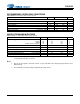


Table Of Contents
- 1. Pin Descriptions
- 2. Typical Connection Diagram
- 3. Characteristic and Specifications
- Recommended Operating Conditions
- Absolute Maximum Ratings
- Analog Input Characteristics
- ADC Digital Filter Characteristics
- Analog Output Characteristics
- Analog Passthrough Characteristics
- PWM Output Characteristics
- Headphone Output Power Characteristics
- Line Output Voltage Level Characteristics
- Combined DAC Interpolation and onChip Analog FIlter Response
- Switching Specifications - Serial Port
- Switching Specifications - I²C Control Port
- DC Electrical Characteristics
- Digital Interface Specifications and Characteristics
- Power Consumption
- 4. Applications
- 4.1 Overview
- 4.2 Analog Inputs
- 4.3 Analog Outputs
- 4.4 Analog In to Analog Out Passthrough
- 4.5 PWM Outputs
- 4.6 Serial Port Clocking
- 4.7 Digital Interface Formats
- 4.8 Initialization
- 4.9 Recommended Power-up Sequence
- 4.10 Recommended Power-Down Sequence
- 4.11 Required Initialization Settings
- 4.12 Control Port Operation
- 5. Register Quick Reference
- 6. Register Description
- 6.1 Chip I.D. and Revision Register (Address 01h) (Read Only)
- 6.2 Power Control 1 (Address 02h)
- 6.3 Power Control 2 (Address 03h)
- 6.4 Power Control 3 (Address 04h)
- 6.5 Clocking Control (Address 05h)
- 6.6 Interface Control 1 (Address 06h)
- 6.7 Interface Control 2 (Address 07h)
- 6.8 Input x Select: ADCA and PGAA (Address 08h), ADCB and PGAB (Address 09h)
- 6.9 Analog and HPF Control (Address 0Ah)
- 6.10 ADC HPF Corner Frequency (Address 0Bh)
- 6.11 Misc. ADC Control (Address 0Ch)
- 6.12 Playback Control 1 (Address 0Dh)
- 6.13 Miscellaneous Controls (Address 0Eh)
- 6.14 Playback Control 2 (Address 0Fh)
- 6.15 MICx Amp Control:MIC A (Address 10h) and MIC B (Address 11h)
- 6.16 PGAx Vol. and ALCx Transition Ctl.: ALC, PGA A (Address 12h) and ALC, PGA B (Address 13h)
- 6.17 Passthrough x Volume: PASSAVOL (Address 14h) and PASSBVOL (Address 15h)
- 6.18 ADCx Volume Control: ADCAVOL (Address 16h) and ADCBVOL (Address 17h)
- 6.19 ADCx Mixer Volume: ADCA (Address 18h) and ADCB (Address 19h)
- 6.20 PCMx Mixer Volume: PCMA (Address 1Ah) and PCMB (Address 1Bh)
- 6.21 Beep Frequency and On Time (Address 1Ch)
- 6.22 Beep Volume and Off Time (Address 1Dh)
- 6.23 Beep and Tone Configuration (Address 1Eh)
- 6.24 Tone Control (Address 1Fh)
- 6.25 Master Volume Control: MSTA (Address 20h) and MSTB (Address 21h)
- 6.26 Headphone Volume Control: HPA (Address 22h) and HPB (Address 23h)
- 6.27 Speaker Volume Control: SPKA (Address 24h) and SPKB (Address 25h)
- 6.28 ADC and PCM Channel Mixer (Address 26h)
- 6.29 Limiter Control 1, Min/Max Thresholds (Address 27h)
- 6.30 Limiter Control 2, Release Rate (Address 28h)
- 6.31 Limiter Attack Rate (Address 29h)
- 6.32 ALC Enable and Attack Rate (Address 2Ah)
- 6.33 ALC Release Rate (Address 2Bh)
- 6.34 ALC Threshold (Address 2Ch)
- 6.35 Noise Gate Control (Address 2Dh)
- 6.36 Status (Address 2Eh) (Read Only)
- 6.37 Battery Compensation (Address 2Fh)
- 6.38 VP Battery Level (Address 30h) (Read Only)
- 6.39 Speaker Status (Address 31h) (Read Only)
- 6.40 Charge Pump Frequency (Address 34h)
- 7. Analog Performance Plots
- 8. Example System Clock Frequencies
- 9. PCB Layout Considerations
- 10. ADC and DAC Digital Filters
- 11. Parameter Definitions
- 12. Package Dimensions
- 13. Ordering Information
- 14. References
- 15. Revision History
DS680F2 13
CS42L52
3/1/13
ANALOG INPUT CHARACTERISTICS
Test Conditions (unless otherwise specified): Input sine wave (relative to digital full scale): 1 kHz through passive input filter; All
Supplies = VA; T
A
= +25C; Sample Frequency = 48 kHz; Measurement Bandwidth is 20 Hz to 20 kHz unless otherwise speci-
fied; “Required Initialization Settings” on page 37 written on power up.
3. Measured with DAC delivering full-scale output into specified load.
4. Measured between analog input and AGND.
VA = 2.5V VA = 1.8V
Parameters Min Typ Max Min Typ Max Unit
Analog In to ADC (PGA bypassed)
Dynamic Range A-weighted
unweighted
93
90
99
96
-
-
90
87
96
93
-
-
dB
dB
Total Harmonic Distortion + Noise -1 dBFS
-20 dBFS
-60 dBFS
-
-
-
-86
-76
-36
-80
-
-30
-
-
-
-84
-73
-33
-78
-
-27
dB
dB
dB
Analog In to PGA to ADC
Dynamic Range
PGA Setting: 0 dB A-weighted
unweighted
92
89
96
93
-
-
89
86
95
92
-
-
dB
dB
PGA Setting: +12 dB A-weighted
unweighted
85
82
91
88
-
-
82
79
88
85
-
-
dB
dB
Total Harmonic Distortion + Noise
PGA Setting: 0 dB -1 dBFS
-60 dBFS
-
-
-88
-33
-82
-27
-
-
-86
-32
-80
-26
dB
dB
PGA Setting: +12 dB -1 dBFS - -85 -79 - -83 -77 dB
Analog In to MIC Pre-Amp (+16 dB) to PGA to ADC
Dynamic Range
PGA Setting: 0 dB A-weighted
unweighted
-
-
86
83
-
-
-
-
83
80
-
-
dB
dB
Total Harmonic Distortion + Noise
PGA Setting: 0 dB -1 dBFS - -76 - - -74 - dB
Analog In to MIC Pre-Amp (+32 dB) to PGA to ADC
Dynamic Range
PGA Setting: 0 dB A-weighted
unweighted
-
-
76
73
-
-
-
-
74
71
-
-
dB
dB
Total Harmonic Distortion + Noise
PGA Setting: 0 dB -2 dBFS - -74 - - -71 - dB
Other Characteristics
DC Accuracy
Interchannel Gain Mismatch - 0.2 - - 0.2 - dB
Gain Drift - ±100 - - ±100 - ppm/°C
Offset Error SDOUT Code with HPF On - 352 - - 352 - LSB
Input
Interchannel Isolation - 90 - - 90 - dB
HP Amp to Analog Input Isolation R
L
= 10 k
(Note 3) R
L
= 16
-
-
100
70
-
-
-
-
100
70
-
-
dB
dB
Speaker Amp to Analog Input Isolation - 60 - - 60 - dB
Full-scale Input Voltage ADC
PGA (0 dB)
PGA (+12 dB)
MIC (+16 dB)
MIC (+32 dB)
0.73•VA
0.73•VA
0.769•VA
0.770•VA
0.194•VA
0.115•VA
0.019•VA
0.83•VA
0.83•VA
0.73•VA
0.73•VA
0.769•VA
0.770•VA
0.194•VA
0.115•VA
0.019•VA
0.83•VA
0.83•VA
Vpp
Vpp
Vpp
Vpp
Vpp
Input Impedance (Note 4) ADC
PGA
MIC
-
-
-
20
39
50
-
-
-
-
-
-
20
39
50
-
-
-
k
k
k