
User Manual


Table Of Contents
- 1. Pin Descriptions
- 2. Typical Connection Diagram
- 3. Characteristic and Specifications
- Recommended Operating Conditions
- Absolute Maximum Ratings
- Analog Input Characteristics
- ADC Digital Filter Characteristics
- Analog Output Characteristics
- Analog Passthrough Characteristics
- PWM Output Characteristics
- Headphone Output Power Characteristics
- Line Output Voltage Level Characteristics
- Combined DAC Interpolation and onChip Analog FIlter Response
- Switching Specifications - Serial Port
- Switching Specifications - I²C Control Port
- DC Electrical Characteristics
- Digital Interface Specifications and Characteristics
- Power Consumption
- 4. Applications
- 4.1 Overview
- 4.2 Analog Inputs
- 4.3 Analog Outputs
- 4.4 Analog In to Analog Out Passthrough
- 4.5 PWM Outputs
- 4.6 Serial Port Clocking
- 4.7 Digital Interface Formats
- 4.8 Initialization
- 4.9 Recommended Power-up Sequence
- 4.10 Recommended Power-Down Sequence
- 4.11 Required Initialization Settings
- 4.12 Control Port Operation
- 5. Register Quick Reference
- 6. Register Description
- 6.1 Chip I.D. and Revision Register (Address 01h) (Read Only)
- 6.2 Power Control 1 (Address 02h)
- 6.3 Power Control 2 (Address 03h)
- 6.4 Power Control 3 (Address 04h)
- 6.5 Clocking Control (Address 05h)
- 6.6 Interface Control 1 (Address 06h)
- 6.7 Interface Control 2 (Address 07h)
- 6.8 Input x Select: ADCA and PGAA (Address 08h), ADCB and PGAB (Address 09h)
- 6.9 Analog and HPF Control (Address 0Ah)
- 6.10 ADC HPF Corner Frequency (Address 0Bh)
- 6.11 Misc. ADC Control (Address 0Ch)
- 6.12 Playback Control 1 (Address 0Dh)
- 6.13 Miscellaneous Controls (Address 0Eh)
- 6.14 Playback Control 2 (Address 0Fh)
- 6.15 MICx Amp Control:MIC A (Address 10h) and MIC B (Address 11h)
- 6.16 PGAx Vol. and ALCx Transition Ctl.: ALC, PGA A (Address 12h) and ALC, PGA B (Address 13h)
- 6.17 Passthrough x Volume: PASSAVOL (Address 14h) and PASSBVOL (Address 15h)
- 6.18 ADCx Volume Control: ADCAVOL (Address 16h) and ADCBVOL (Address 17h)
- 6.19 ADCx Mixer Volume: ADCA (Address 18h) and ADCB (Address 19h)
- 6.20 PCMx Mixer Volume: PCMA (Address 1Ah) and PCMB (Address 1Bh)
- 6.21 Beep Frequency and On Time (Address 1Ch)
- 6.22 Beep Volume and Off Time (Address 1Dh)
- 6.23 Beep and Tone Configuration (Address 1Eh)
- 6.24 Tone Control (Address 1Fh)
- 6.25 Master Volume Control: MSTA (Address 20h) and MSTB (Address 21h)
- 6.26 Headphone Volume Control: HPA (Address 22h) and HPB (Address 23h)
- 6.27 Speaker Volume Control: SPKA (Address 24h) and SPKB (Address 25h)
- 6.28 ADC and PCM Channel Mixer (Address 26h)
- 6.29 Limiter Control 1, Min/Max Thresholds (Address 27h)
- 6.30 Limiter Control 2, Release Rate (Address 28h)
- 6.31 Limiter Attack Rate (Address 29h)
- 6.32 ALC Enable and Attack Rate (Address 2Ah)
- 6.33 ALC Release Rate (Address 2Bh)
- 6.34 ALC Threshold (Address 2Ch)
- 6.35 Noise Gate Control (Address 2Dh)
- 6.36 Status (Address 2Eh) (Read Only)
- 6.37 Battery Compensation (Address 2Fh)
- 6.38 VP Battery Level (Address 30h) (Read Only)
- 6.39 Speaker Status (Address 31h) (Read Only)
- 6.40 Charge Pump Frequency (Address 34h)
- 7. Analog Performance Plots
- 8. Example System Clock Frequencies
- 9. PCB Layout Considerations
- 10. ADC and DAC Digital Filters
- 11. Parameter Definitions
- 12. Package Dimensions
- 13. Ordering Information
- 14. References
- 15. Revision History
DS680F2 11
CS42L52
3/1/13
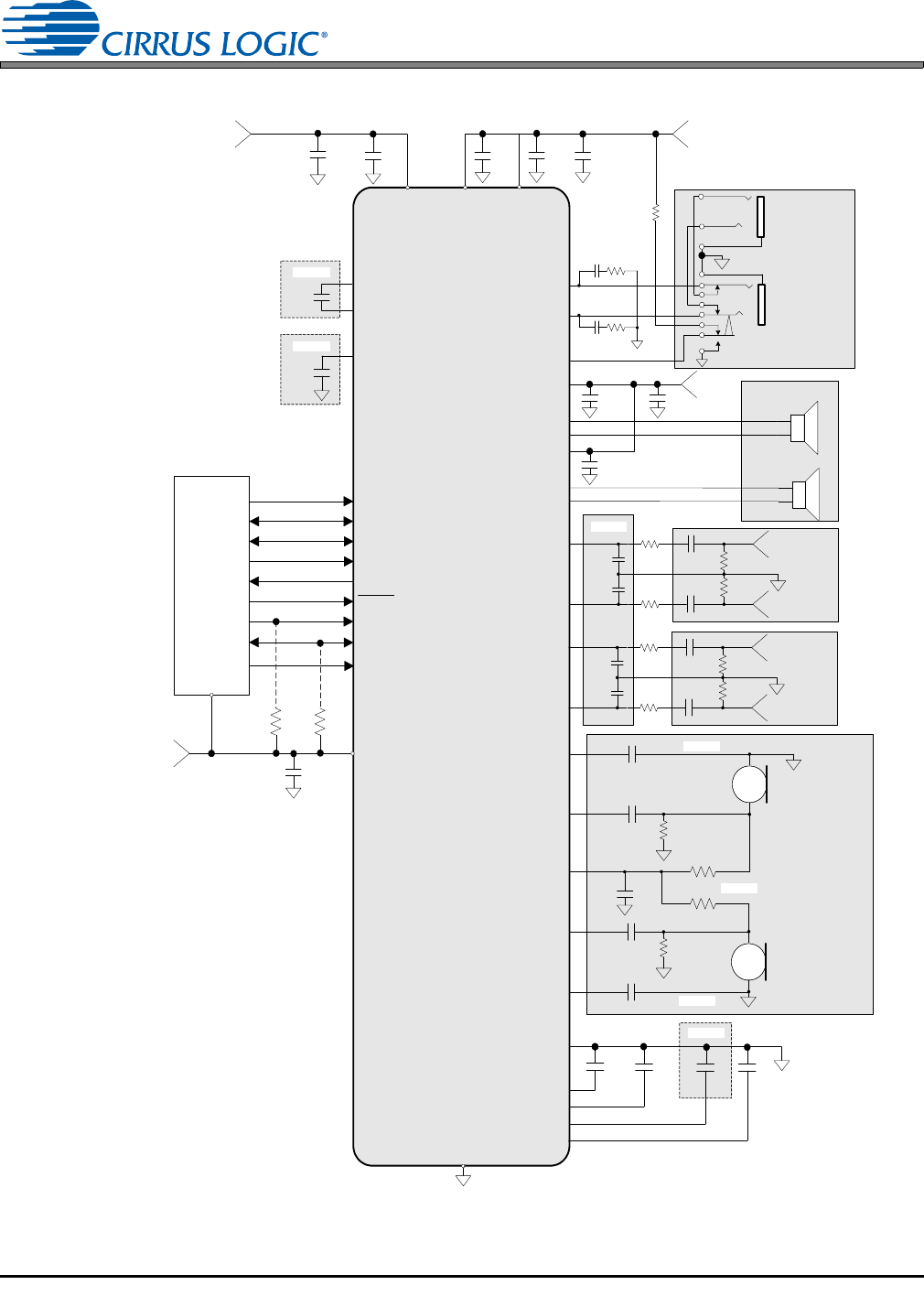
2. TYPICAL CONNECTION DIAGRAM
Note 4
Note 3
Note 2
Note 1
1 µF
+1.8 V to +2.5 V
0.1 µF
1 µF
DGND
VL
0.1 µF
+1.8 V to +3.3 V
SCL
SDA
RESET
2 k
LRCK
Digital Audio
Processor
MCLK
SCLK
VD
MIC1-
AIN3A/MIC1A
Microphone 1
SDIN
SDOUT
CS42L52
2 k
MICBIAS
+1.8 V to +2.5 V
HP/LINE_OUTB
HP/LINE_OUTA
AIN1A
Left 1
1800 pF
1800 pF
100 k
100
AIN1B
Right 1
*
*
R
L
0.1 µF
VA
Headphone Out
Left & Right
Line Level Out
Left & Right
FLYP
FLYN
-VHPFILT
0.1 µF
51.1
0.022 µF
100 k
100
SPKR_OUTA+
SPKR_OUTA-
SPKR/HP
51.1
0.022 µF
MIC1+
AIN4A/MIC2A
MIC2+
AIN4B/MIC2B
Microphone 2
MIC2-
AIN3B/MIC1B
100 k
R
L
100 k
1 µF
1 µF
0.1 µF
+VHP
1 µF
10 µF
VQ
AGND
* Capacitors must be C0G or equivalent
150 pF
AFILTA
AFILTB
150 pF
1 µF
**
FILT+
1 µF
1 µF
1 µF
1 µF
* *Use low ESR ceramic capacitors.
**
**
See Note 5
SPKR_OUTB+
SPKR_OUTB-
1 µF
VP
VP
+1.6 V to
+5 V
Stereo Speakers
AIN2A
Left 2
1800 pF
1800 pF
100 k
100
AIN2B
Right 2
*
*
100 k
100
1 µF
1 µF
0.1 µF
0.1 µF
Analog
Input 1
Analog
Input 2
10 µF
Mic-Level
Inputs
47 k
Notes:
1. Recommended values for the default charge pump switching
frequency. The required capacitance follows an inverse
relationship with the charge pump’s switching frequency. When
increasing the switching frequency, the capacitance may
decrease; when lowering the switching frequency, the
capacitance must increase.
2. Larger capacitance reduces the ripple on the internal
amplifier’s supply. This may reduce the distortion at higher
output power levels.
3. Additional bulk capacitance may be added to improve PSRR
at low frequencies.
4. These capacitors serve as a charge reservoir for the internal
switched capacitor ADC modulators. They are only needed
when the PGA (Programmable Gain Amplifier) is bypassed.
5. Series resistance in the path of the power supplies must be
avoided. Any voltage drop on VHP will directly impact the
negative charge pump supply (-VHPFILT) and clip the audio
output.
6. The value of R
L
, a current-limiting resistor used with electret
condenser microphones, is dictated by the microphone
cartridge.
7. The negative terminal of the MICx inputs connects to the
ground pin of the microphone cartridge. Gain is applied only to
the positive terminal.
Note 6
Note 7
Note 7
AD0
Figure 1. Typical Connection Diagram