DRAFTv1 3/1/13 CS42L52 Low-Power, Stereo CODEC with Headphone and Speaker Amps Stereo CODEC Class D Stereo/Mono Speaker Amplifier High Performance Stereo ADC and DAC – 99 dB (ADC), 98 dB (DAC) Dyn. Range (A-wtd) – -88 dB THD+N No External Filter Required High-power Stereo Output at 10% THD+N – 2 x 1.00 W into 8 @ 5.0 V – 2 x 550 mW into 8 @ 3.7 V – 2 x 230 mW into 8 @ 2.
3/1/13 CS42L52 System Features General Description 12, 24, and 27 MHz Master Clock Support in The CS42L52 is a highly integrated, low-power stereo CODEC with headphone and Class D speaker amplifiers. The CS42L52 offers many features suitable for low-power, portable system applications.
/1/13 CS42L52 TABLE OF CONTENTS 1. PIN DESCRIPTIONS .............................................................................................................................. 8 1.1 I/O Pin Characteristics .................................................................................................................... 10 2. TYPICAL CONNECTION DIAGRAM ................................................................................................... 11 3. CHARACTERISTIC AND SPECIFICATIONS ............
3/1/13 CS42L52 4.12.2.1 Map Increment (INCR) ............................................................................................. 39 5. REGISTER QUICK REFERENCE ........................................................................................................ 40 6. REGISTER DESCRIPTION .................................................................................................................. 42 6.1 Chip I.D. and Revision Register (Address 01h) (Read Only) ..............................
3/1/13 CS42L52 6.12 Playback Control 1 (Address 0Dh) ............................................................................................... 51 6.12.1 Headphone Analog Gain ..................................................................................................... 51 6.12.2 Playback Volume Setting B=A ............................................................................................ 51 6.12.3 Invert PCM Signal Polarity .............................................................
3/1/13 CS42L52 6.25.1 Master Volume Control ........................................................................................................ 63 6.26 Headphone Volume Control: HPA (Address 22h) and HPB (Address 23h) ................................. 63 6.26.1 Headphone Volume Control ................................................................................................ 63 6.27 Speaker Volume Control: SPKA (Address 24h) and SPKB (Address 25h) .................................. 64 6.27.
3/1/13 CS42L52 9.1 Power Supply and Grounding ......................................................................................................... 77 9.2 QFN Thermal Pad .......................................................................................................................... 77 10. ADC AND DAC DIGITAL FILTERS .................................................................................................. 78 11. PARAMETER DEFINITIONS ...................................................
3/1/13 CS42L52 SDOUT DGND VD VL RESET SPKR/HP 36 35 34 33 32 31 MCLK 37 SDIN SCLK 39 38 LRCK SDA 1 30 AIN1B SCL 2 29 AIN1A AD0 3 28 AFILTB SPKR_OUTA+ 4 27 AFILTA VP 5 26 AIN2B SPKR_OUTA- 6 25 AIN2A SPKR_OUTB+ 7 24 AIN3B/MIC2-/MIC1B VP 8 23 AIN3A/MIC1-/MIC1A SPKR_OUTB- 9 22 AIN4B/MIC2+/MIC2B -VHPFILT 10 21 AIN4A/MIC1+/MIC2A Pin Name SDA SCL AD0 SPKR_OUTA+ SPKR_OUTASPKR_OUTB+ SPKR_OUTBVP -VHPFILT FLYN FLYP +VHP HP/LINE_OUTB, A VA 8 40 1.
3/1/13 CS42L52 AGND 17 FILT+ 18 VQ 19 MICBIAS 20 AIN4A,B AIN3A,B MIC1+,MIC2+,MIC2A,B MIC1A,B AIN2A,B AIN1A,B AFILTA,B 21,22 23,24 21,23 22,24 21,22 23,24 25,26 29,30 27,28 SPKR/HP 31 RESET 32 VL 33 VD DGND SDOUT MCLK SCLK SDIN 34 35 36 37 38 39 LRCK 40 GND/Thermal Pad DS680F2 - Analog Ground (Input) - Ground reference for the internal analog section. Positive Voltage Reference (Output) - Positive reference voltage for the internal sampling circuits.
3/1/13 CS42L52 1.1 I/O Pin Characteristics Input and output levels and associated power supply voltage are shown in the table below. Logic levels should not exceed the corresponding power supply voltage. Power Supply VL Pin Name I/O Internal Connections Driver Receiver RESET AD0 SCL SDA - 1.65 V - 3.47 V, CMOS/Open Drain 1.65 V - 3.47 V, CMOS 1.65 V - 3.47 V, with Hysteresis 1.65 V - 3.47 V, with Hysteresis 1.65 V - 3.47 V, with Hysteresis 1.65 V - 3.47 V, with Hysteresis 1.65 V - 3.
3/1/13 CS42L52 2. TYPICAL CONNECTION DIAGRAM +1.8 V to +2.5 V +1.8 V to +2.5 V 1 µF 0.1 µF 0.1 µF 0.1 µF 1 µF See Note 5 VD VA +VHP Line Level Out Left & Right 47 k 0.022 µF Note 1 1 µF ** FLYP HP/LINE_OUTB FLYN HP/LINE_OUTA Headphone Out Left & Right 51.1 0.022 µF Note 2 -VHPFILT 1 µF 51.1 SPKR/HP ** CS42L52 VP 0.1 µF 10 µF +1.6 V to Stereo Speakers +5 V SPKR_OUTA+ SPKR_OUTA- * *Use low ESR ceramic capacitors. VP 0.
3/1/13 CS42L52 3. CHARACTERISTIC AND SPECIFICATIONS RECOMMENDED OPERATING CONDITIONS AGND=DGND=0 V, All voltages with respect to ground. Parameters DC Power Supply Analog Headphone Amplifier Speaker Amplifier Digital Serial/Control Port Interface Ambient Temperature Commercial - CNZ Symbol Min Max Units VA +VHP VP VD VL TA 1.65 1.65 1.60 1.65 1.65 -40 2.63 2.63 5.25 2.63 3.47 +85 V V V V V C ABSOLUTE MAXIMUM RATINGS AGND = DGND = 0 V; All voltages with respect to ground.
3/1/13 CS42L52 ANALOG INPUT CHARACTERISTICS Test Conditions (unless otherwise specified): Input sine wave (relative to digital full scale): 1 kHz through passive input filter; All Supplies = VA; TA = +25C; Sample Frequency = 48 kHz; Measurement Bandwidth is 20 Hz to 20 kHz unless otherwise specified; “Required Initialization Settings” on page 37 written on power up. Min VA = 2.5V Typ Max Min VA = 1.
3/1/13 CS42L52 ADC DIGITAL FILTER CHARACTERISTICS Parameters (Note 5) Passband (Frequency Response) to -0.1 dB corner Passband Ripple Min Typ Max Unit 0 - 0.4948 Fs -0.09 - 0.17 dB Stopband 0.6 - - Fs Stopband Attenuation 33 - - dB - 7.6/Fs - s - 3.6 24.2 - Hz Hz Total Group Delay High-Pass Filter Characteristics (48 kHz Fs) Frequency Response Phase Deviation -3.0 dB -0.13 dB - 10 - Deg Passband Ripple @ 20 Hz - - 0.17 dB Filter Settling Time - 105/Fs 0 s 5.
3/1/13 CS42L52 ANALOG OUTPUT CHARACTERISTICS Test conditions (unless otherwise specified): Input test signal is a full-scale 997 Hz sine wave; All Supplies = VA; TA = +25C; Sample Frequency = 48 kHz; Measurement bandwidth is 20 Hz to 20 kHz; Test load RL = 10 k CL = 10 pFfor the line output (see Figure 2); Test load RL = 16 CL = 10 pF (see Figure 2) for the headphone output; HP_GAIN[2:0] = 011; “Required Initialization Settings” on page 37 written on power up. VA = 2.
3/1/13 CS42L52 8. See Figure 2. RL and CL reflect the recommended minimum resistance and maximum capacitance required for the internal op-amp's stability and signal integrity. In this circuit topology, CL will effectively move the band-limiting pole of the amp in the output stage. Increasing this value beyond the recommended 150 pF can cause the internal op-amp to become unstable.
3/1/13 CS42L52 PWM OUTPUT CHARACTERISTICS Test conditions (unless otherwise specified): Input test signal is a full scale 997 Hz signal; MCLK = 12.2880 MHz; Measurement Bandwidth is 20 Hz to 20 kHz; Sample Frequency = 48 kHz; Test load RL = 8 for stereo full-bridge, RL = 4 for mono parallel full-bridge; VD = VL = VA = VHP = 1.8 V; PWM Modulation Index of 0.85; PWM Switch Rate = 384 kHz; “Required Initialization Settings” on page 37 written on power up. (Note 9) Parameters (Note 10) Symbol VP = 5.
3/1/13 CS42L52 Parameters (Note 10) MOSFET On Resistance MOSFET On Resistance Efficiency Output Operating Peak Current VP Input Current During Reset Symbol Conditions RDS(ON) VP = 3.7V, Id = 0.5 A VP = 2.5V, Id = 0.5 A RDS(ON) VP = 5.0 V, PO = 2 x 0.8 W, RL = 8 IPC IVP RESET, pin 32, is held low Min Typ - 640 760 81 0.8 Max Units 1.5 5.0 m m % A µA 9. The PWM driver should be used in captive speaker systems only. 10. Optimal PWM performance is achieved when MCLK > 12 MHz.
3/1/13 CS42L52 LINE OUTPUT VOLTAGE LEVEL CHARACTERISTICS Test conditions (unless otherwise specified): Input test signal is a full-scale 997 Hz sine wave; measurement bandwidth is 20 Hz to 20 kHz; Sample Frequency = 48 kHz; Test load RL = 10 k CL = 10 pF (see Figure 2); “Required Initialization Settings” on page 37 written on power up. Parameters Min VA = 2.5V Typ Max Min 2.15 - 1.41 - VA = 1.8V Typ Unit Max AOUTx Voltage Into RL = 10 k HP_GAIN[2:0] 000 Analog Gain (G) 0.3959 001 0.
3/1/13 CS42L52 SWITCHING SPECIFICATIONS - SERIAL PORT Inputs: Logic 0 = DGND, Logic 1 = VL, SDOUT CLOAD = 15 pF. Parameters Symbol RESET pin Low Pulse Width (Note 14) MCLK Frequency (Note 15) MCLK Duty Cycle Min Max 1 - Units ms (See “Serial Port Clocking” on page 33) 45 55 MHz (See “Serial Port Clocking” on page 33) 45 55 64•Fs 45 55 40 52 20 30 20 20 - kHz (See “Serial Port Clocking” on page 33) 45 55 12.
3/1/13 CS42L52 SWITCHING SPECIFICATIONS - I²C CONTROL PORT Inputs: Logic 0 = DGND, Logic 1 = VL, SDA CL = 30 pF.
3/1/13 CS42L52 DC ELECTRICAL CHARACTERISTICS AGND = 0 V; All voltages with respect to ground. Parameters Min Typ Max Units - 0.5•VA 23 - 1 V k A 1 kHz - 0.5•VA 0.6•VA 0.7•VA 0.8•VA 0.83•VA 0.
3/1/13 CS42L52 POWER CONSUMPTION See (Note 20). Operation PDN_SPKB[1:0] PDN_SPKA[1:0] Typical Current (mA) PDN_HPA[1:0] Power Ctl.
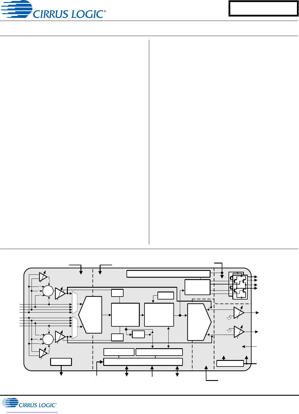
3/1/13 CS42L52 4. APPLICATIONS 4.1 4.1.1 Overview Basic Architecture The CS42L52 is a highly integrated, low-power, 24-bit audio CODEC comprised of a stereo analog-todigital converter (ADC), a stereo digital-to-analog converter (DAC), a digital PWM modulator and two fullbridge power back-ends. The ADC and DAC are designed using multibit delta-sigma techniques - the DAC operates at an oversampling ratio of 128Fs and the ADC operates at 64Fs, where Fs is equal to the system sample rate.
3/1/13 CS42L52 4.
3/1/13 CS42L52 4.2.1 MIC Inputs The input pins 21, 22, 23, and 24 accept stereo line-level or microphone signals. For microphone inputs, either single-ended or differential configuration is allowed, providing programmable pre-amplification of low-level signals. In the single-ended configuration, an internal MUX chooses one of two stereo sets (selection is made independently on channels A and B).
3/1/13 CS42L52 Referenced Control Register Location PGAxVOL[5:0 MAX[2:0], MIN[2:0] “PGAx Vol. and ALCx Transition Ctl.
3/1/13 CS42L52 4.3 Analog Outputs INPUTS FROM ADCA and ADCB Fixed Function DSP AMIXAMUTE AMIXBMUTE AMIXAVOL[6:0] AMIXBVOL[6:0] +12dB/-51.5dB 0.5dB steps PCM Serial Interface VOL PMIXAMUTE PMIXBMUTE PMIXAVOL[6:0] PMIXBVOL[6:0] Channel Swap DEEMPH VOL Channel Swap INV_PCMA INV_PCMB Limiter ADCASWAP[1:0] ADCBSWAP[1:0] Peak Detect PWM Modulator 0dB/-50dB 2.
3/1/13 CS42L52 BATTCMP VPREF[3:0] VPLVL[7:0] SPKAMUTE SPKBMUTE MUTE50/50 SPKMONO SPKSWAP SPKB=A SPKAVOL[7:0] SPKBVOL[7:0] +0dB/-102dB 0.5dB steps from DSP Engine from DSP Engine VOL PWM Modulator + A + B - Gate Drive Short Circuit SPKASHRT SPKBSHRT Figure 11. PWM Output Stage Referenced Control Register Location PWM Control SPKxMUTE ......................... MUTE50/50 ......................... SPKMONO .......................... SPKxVOL[7:0] ..................... SPKSWAP...........................
3/1/13 CS42L52 BEEP[1:0] = '11' CONTINUOUS BEEP: Beep turns on at a configurable frequency (FREQ) and volume (BPVOL) and remains on until BEEP is cleared. BEEP[1:0] = '10' MULTI-BEEP: Beep turns on at a configurable frequency (FREQ) and volume (BPVOL) for the duration of ONTIME and turns off for the duration of OFFTIME. On and off cycles are repeated until BEEP is cleared. BEEP[1:0] = '01' SINGLE-BEEP: Beep turns on at a configurable frequency (FREQ) and volume (BPVOL) for the duration of ONTIME.
3/1/13 CS42L52 In p u t M A X [2 :0 ] L im ite r A T T A C K /R E L E A S E S O U N D C U S H IO N V o lu m e O u tp u t (a fte r L im ite r) C U S H [2 :0 ] M A X [2 :0 ] A R A T E [5 :0 ] R R A T E [5 :0 ] Figure 14. Peak Detect and Limiter 4.4 Analog In to Analog Out Passthrough The CS42L52 accommodates analog routing of the analog input signal directly to the headphone amplifiers.
3/1/13 CS42L52 4.4.2 Referenced Control Register Location PDN_ADCx ......................... PASSTHRU......................... PDN_OVRD ........................ SPKx_PDN[1:0]...................
3/1/13 CS42L52 4.5.2 VP Battery Compensation The CS42L52 provides the option to maintain a desired power output level, independent of the VP supply. When enabled, this feature works by monitoring the voltage on the VP supply and reducing the attenuation on the speaker outputs when VP voltage levels fall. Note: The internal ADC that monitors the VP supply operates from the VA supply. Calculations are based on typical VA levels of 1.8 V and 2.5 V using the VPREF bits. 4.5.2.
3/1/13 CS42L52 input master clock (MCLK) in Master Mode. Refer to the tables below for the required setting in register 05h and 06h associated with a given MCLK and sample rate. Referenced Control Register Location M/S Register 05h Register 06h “Master/Slave Mode” on page 46 “Clocking Control (Address 05h)” on page 44 “Interface Control 1 (Address 06h)” on page 46 MCLK (MHz) 12.2880 11.2896 18.4320 (Slave Mode ONLY) 16.9344 (Slave Mode ONLY) 12.0000 24.0000 Sample Rate, Fs (kHz) 8.0000 12.
3/1/13 CS42L52 MCLK (MHz) 27.0000 Sample Rate, Fs (kHz) 8.0000 12.0000 24.0000 32.0000 44.1176 48.0000 11.0294 22.0588 16.0000 SPEED[1:0] (AUTO=’0’b) 11 11 10 01 01 01 11 10 10 32kGROUP VIDEOCLK RATIO[1:0] MCLKDIV2 1 0 0 1 0 0 0 0 1 1 1 1 1 1 1 1 1 1 01 01 01 01 11 01 11 11 01 0 0 0 0 0 0 0 0 0 Table 1. MCLK, LRCK Quick Decode 4.
3/1/13 CS42L52 1/fs LRCK SCLK SDIN L eft C h a n n el L SB MSB R ig ht C h a n n el LS B M SB HP/LINE OUTA LSB M SB HP/LINE OUTB Audio Word Length (AWL) Figure 19. DSP Mode Format) When configuring the 16-bit SDOUT word length with an 8 kHz sample rate in master mode and when SCLK is set equal to MCLK, perform the following write sequences: Register commands ONLY when entering DSP 16-bit, 8 kHz Fs, SCLK=MCLK, master mode: 1 2 Register[Bits] Value 0x0C[1:0] 0x03 Refer to Section 4.
3/1/13 CS42L52 4.9 Recommended Power-up Sequence 1. Hold RESET low until the power supplies are stable. 2. Bring RESET high. 3. The default state of the PDN bit is 1. Load the desired register settings while keeping the PDN bit set to 11. 4. Load the required initialization settings listed in Section 4.11. 5. Apply MCLK at the appropriate frequency, as discussed in Section 4.6. SCLK may be applied or set to master at any time; LRCK may only be applied or set to master while the PDN bit is set to 1. 6.
3/1/13 CS42L52 1. Write 0x99 to register 0x00. 2. Write 0xBA to register 0x3E. 3. Write 0x80 to register 0x47. 4. Write 1 to bit 7 in register 0x32. 5. Write 00 to bit 7 in register 0x32. 6. Write 0x00 to register 0x00. 4.12 Control Port Operation The control port is used to access the registers, allowing the CODEC to be configured for the desired operational modes and formats. The operation of the control port may be completely asynchronous with respect to the audio sample rates.
3/1/13 CS42L52 0 1 2 3 4 5 6 7 8 9 10 11 12 13 14 15 16 17 18 19 20 21 22 23 24 25 26 27 28 SCL CHIP ADDRESS (WRITE) SDA 1 0 0 1 STOP MAP BYTE 0 1 AD0 0 INCR 6 5 4 3 2 1 ACK CHIP ADDRESS (READ) 1 0 ACK START 0 0 1 0 DATA 1 AD0 1 7 ACK START DATA +1 0 7 ACK 0 DATA + n 7 0 NO ACK STOP Figure 21. Control Port Timing, I²C Read Since the read operation cannot set the MAP, an aborted write operation is used as a preamble.
3/1/13 CS42L52 5. REGISTER QUICK REFERENCE Default values are shown below the bit names. Unless otherwise specified, all “Reserved” bits must maintain their default values. Adr.
3/1/13 CS42L52 Adr. 1Bh p 58 1Ch p 59 1Dh p 60 1Eh p 61 1Fh p 62 20h p 63 21h p 63 22h p 63 23h p 63 24h p 64 25h p 64 26h p 64 27h p 65 28h p 66 29h p 67 2Ah p 67 2Bh p 68 2Ch p 68 2Dh p 69 2Eh p 70 2Fh p 71 30h p 72 31h p 72 32h Function PCMMIXB Vol 7 PMIXBMUTE 0 BEEP Freq, FREQ3 On Time 0 BEEP Vol, OFFTIME2 Off Time 0 BEEP, BEEP1 Tone Cfg.
3/1/13 CS42L52 6. REGISTER DESCRIPTION All registers are read/write except for the Chip I.D. and Revision Register and Interrupt Status Register, which are read only. See the following bit definition tables for bit assignment information. The default state of each bit after a power-up sequence or reset is listed in each bit description. Unless otherwise specified, all “Reserved” bits must maintain their default value. 6.1 Chip I.D. and Revision Register (Address 01h) (Read Only) 7 CHIPID4 6.1.
3/1/13 CS42L52 input path. The PGAxSEL bits may be used to isolate the input signal(s) from the PGA outputs. When the PGA is powered down, no input should be selected. Refer to “ADC Input Select” on page 48 and “PGA Input Mapping” on page 49 for the required settings. 6.2.3 Power Down ADCx Configures the power state of ADC channel x. PDN_ADCx ADC Status 0 Powered Up 1 Powered Down Application “Analog In to Analog Out Passthrough” on page 31 Notes: 1.
3/1/13 CS42L52 6.4 Power Control 3 (Address 04h) 7 PDN_HPB1 6.4.1 6 PDN_HPB0 5 PDN_HPA1 4 PDN_HPA0 3 PDN_SPKB1 2 PDN_SPKB0 1 PDN_SPKA1 0 PDN_SPKA0 Headphone Power Control Configures how the SPKR/HP pin, 31, controls the power for the headphone amplifier. 6.4.2 PDN_HPx[1:0] Headphone Status 00 Headphone channel is ON when the SPKR/HP pin, 31, is LO. Headphone channel is OFF when the SPKR/HP pin, 31, is HI. 01 Headphone channel is ON when the SPKR/HP pin, 31, is HI.
3/1/13 CS42L52 6.5.2 Speed Mode Configures the speed mode of the CODEC in slave mode and sets the appropriate MCLK divide ratio for LRCK and SCLK in master mode. SPEED[1:0] Slave Mode Master Mode Serial Port Speed MCLK/LRCK Ratio SCLK/LRCK Ratio 00 Double-Speed Mode (DSM - 50 kHz -100 kHz Fs) 128 64 01 Single-Speed Mode (SSM - 4 kHz -50 kHz Fs) 256 64 10 Half-Speed Mode (HSM - 12.5kHz -25 kHz Fs) 512 64 11 Quarter-Speed Mode (QSM - 4 kHz -12.
3/1/13 CS42L52 6.5.6 MCLK Divide By 2 Divides the input MCLK by 2 prior to all internal circuitry. MCLKDIV2 No divide 1 Divided by 2 Application: “Serial Port Clocking” on page 33 Note: 6.6 MCLK signal into CODEC 0 In slave mode, this bit is ignored when the AUTO bit (“Auto-Detect” on page 44) is disabled. Interface Control 1 (Address 06h) 7 M/S 6.6.1 6 INV_SCLK 5 ADCDIF 4 DSP 3 DACDIF1 2 DACDIF0 1 AWL1 0 AWL0 Master/Slave Mode Configures the serial port I/O clocking. M/S 6.6.
3/1/13 CS42L52 6.6.5 DAC Interface Format Configures the digital interface format for data on SDIN. DACDIF[1:0] DAC Interface Format 00 Left Justified, up to 24-bit data 01 I²S, up to 24-bit data 10 Right Justified 11 Reserved Application: “Digital Interface Formats” on page 35 Note: Select the audio word length for Right Justified using the AWL[1:0] bits (“Audio Word Length” on page 47). 6.6.
3/1/13 CS42L52 6.7.3 Tri-State Serial Port Interface Determines the state of the serial port drivers. 3ST_SP Serial Port Status Slave Mode Master Mode 0 Serial Port clocks are inputs and SDOUT is output Serial Port clocks and SDOUT are outputs 1 Serial Port clocks are inputs and SDOUT is HI-Z Serial Port clocks and SDOUT are HI-Z Notes: 1. Slave/Master Mode is determined by the M/S bit in “Master/Slave Mode” on page 46. 2.
3/1/13 CS42L52 6.8.2 PGA Input Mapping Selects one or sums/mixes the analog input signal into the PGA. Each bit of the PGAx_SEL[5:1] word corresponds to individual channels (i.e. PGAx_SEL1 selects AIN1x, PGAx_SEL2 selects AIN2x, etc.).
3/1/13 CS42L52 6.10 ADC HPF Corner Frequency (Address 0Bh) 7 Reserved 6 Reserved 5 Reserved 4 Reserved 3 HPFB_CF1 2 HPFB_CF0 1 HPFA_CF1 0 HPFA_CF0 6.10.1 HPF x Corner Frequency Sets the corner frequency (-3 dB point) for the internal High-Pass Filter (HPF). 6.11 HPFx_CF[1:0] HPF Corner Frequency Setting (Fs=48 kHz) 00 Normal setting as specified in “ADC Digital Filter Characteristics” on page 14 01 119 Hz 10 236 Hz 11 464 Hz Misc. ADC Control (Address 0Ch) 7 ADCB=A 6.11.
3/1/13 CS42L52 6.11.4 Invert ADC Signal Polarity Configures the polarity of the ADC signal. 6.11.5 INV_ADCx ADC Signal Polarity 0 Not Inverted 1 Inverted ADC Mute Configures a digital mute on ADC channel x. ADCxMUTE 0 Disabled 1 Enabled Note: 6.12 ADC Mute When the ADCxMUTE bit is enabled, the PGA will automatically apply 6 dB of attenuation. Playback Control 1 (Address 0Dh) 7 HPGAIN2 6 HPGAIN1 5 HPGAIN0 4 PLYBCKB=A 3 INV_PCMB 2 INV_PCMA 1 MSTBMUTE 0 MSTAMUTE 6.12.
3/1/13 CS42L52 6.12.3 Invert PCM Signal Polarity Configures the polarity of the digital input signal. INV_PCMx PCM Signal Polarity 0 Not Inverted 1 Inverted 6.12.4 Master Playback Mute Configures a digital mute on the master volume control for channel x. MSTxMUTE Master Mute 0 Not Inverted 1 Inverted Note: The muting function is affected by the DIGSFT (“Digital Soft Ramp” on page 53) and DIGZC (“Digital Zero Cross” on page 53) bits. 6.
3/1/13 CS42L52 Using this bit before the relevant circuitry begins normal operation could cause the change to take effect immediately, ignoring the FREEZE bit. 6.13.4 HP/Speaker De-emphasis Configures a 15s/50s digital de-emphasis filter response on the headphone/line and speaker outputs. DEEMPHASIS Control Port Status 0 Disabled 1 Enabled 6.13.5 Digital Soft Ramp Configures an incremental volume ramp from the current level to the new level at the specified rate.
3/1/13 CS42L52 6.14 Playback Control 2 (Address 0Fh) 7 HPBMUTE 6 HPAMUTE 5 SPKBMUTE 4 SPKAMUTE 3 SPKB=A 2 SPKSWAP 1 SPKMONO 0 MUTE50/50 6.14.1 Headphone Mute Configures a digital mute on headphone channel x. HPxMUTE Headphone Mute 0 Disabled 1 Enabled 6.14.2 Speaker Mute Configures a digital mute on speaker channel x. SPKxMUTE Speaker Mute 0 Disabled 1 Enabled 6.14.3 Speaker Volume Setting B=A Configures independent or ganged volume control of the speaker output.
3/1/13 CS42L52 6.15 MICx Amp Control:MIC A (Address 10h) and MIC B (Address 11h) 7 Reserved 6 MICxSEL 5 MICxCFG 4 MICxGAIN4 3 MICxGAIN3 2 MICxGAIN2 1 MICxGAIN1 0 MICxGAIN0 1 PGAxVOL1 0 PGAxVOL0 6.15.1 MIC x Select Selects one of two single-ended MIC inputs on channel x. MICxSEL MIC x Selection 0 MIC 1x 1 MIC 2x Application: “MIC Inputs” on page 26 6.15.2 MICx Configuration Configures the input topology for MICx.
3/1/13 CS42L52 6.16.2 ALCx Zero Cross Disable Configures an override of the analog zero cross setting. ALCxZCDIS ALC Zero Cross Disable 0 OFF; ALC Attack Rate is dictated by the ANLGZC (“Ch. x Analog Zero Cross” on page 49) setting 1 ON; ALC volume changes take effect at any time, regardless of the ANLGZC setting. Application: “Automatic Level Control (ALC)” on page 26 6.16.3 PGAx Volume Sets the volume/gain of the Programmable Gain Amplifier (PGA). PGAxVOL[5:0] Volume 01 1111 12 dB ... ...
3/1/13 CS42L52 6.17 Passthrough x Volume: PASSAVOL (Address 14h) and PASSBVOL (Address 15h) 7 PASSxVOL7 6 PASSxVOL6 5 PASSxVOL5 4 PASSxVOL4 3 PASSxVOL3 2 PASSxVOL2 1 PASSxVOL1 0 PASSxVOL0 6.17.1 Passthrough x Volume Sets the volume/gain of the signal routed from the PGA to the headphone/line output. PASSxVOL[7:0] Gain 0111 1111 12 dB ... ... 0001 1000 12 dB ... ... 0000 0001 +0.5 dB 0000 0000 0 dB 11111 1111 -0.5 dB ... ... 1000 1000 -60.0 dB ... ... 1000 0000 -60.
3/1/13 CS42L52 6.19 ADCx Mixer Volume: ADCA (Address 18h) and ADCB (Address 19h) 7 AMIXxMUTE 6 AMIXxVOL6 5 AMIXxVOL5 4 AMIXxVOL4 3 AMIXxVOL3 2 AMIXxVOL2 1 AMIXxVOL1 0 AMIXxVOL0 6.19.1 ADC Mixer Channel x Mute Configures a digital mute on the ADC mix in the DSP. AMIXxMUTE ADC Mixer Mute 0 Disabled 1 Enabled 6.19.2 ADC Mixer Channel x Volume Sets the volume/gain of the ADC mix in the DSP. 6.20 AMIXxVOL[6:0] Volume 001 1000 +12.0 dB ... ... 000 0001 +0.
3/1/13 CS42L52 6.21 Beep Frequency and On Time (Address 1Ch) 7 FREQ3 6 FREQ2 5 FREQ1 4 FREQ0 3 ONTIME3 2 ONTIME2 1 ONTIME1 0 ONTIME0 6.21.1 Beep Frequency Sets the frequency of the beep signal. FREQ[3:0] Frequency (Fs = 12, 24, 48 or 96 kHz) Pitch 0000 260.87 Hz C4 0001 521.74 Hz C5 0010 585.37 Hz D5 0011 666.67 Hz E5 0100 705.88 Hz F5 0101 774.19 Hz G5 0110 888.89 Hz A5 0111 1000.00 Hz B5 1000 1043.48 Hz C6 1001 1200.00 Hz D6 1010 1333.33 Hz E6 1011 1411.
3/1/13 CS42L52 6.21.2 Beep On Time Sets the on duration of the beep signal. ONTIME[3:0] On Time (Fs = 12, 24, 48 or 96 kHz) 0000 ~86 ms 0001 ~430 ms 0010 ~780 ms 0011 ~1.20 s 0100 ~1.50 s 0101 ~1.80 s 0110 ~2.20 s 0111 ~2.50 s 1000 ~2.80 s 1001 ~3.20 s 1010 ~3.50 s 1011 ~3.80 s 1100 ~4.20 s 1101 ~4.50 s 1110 ~4.80 s 1111 ~5.20 s Application: “Beep Generator” on page 29 Notes: 1. This setting must not change when BEEP is enabled. 2.
3/1/13 CS42L52 6.22.2 Beep Volume Sets the volume of the beep signal. BEEPVOL[4:0] Gain 00110 +6.0 dB ··· ··· 00000 -6 dB 11111 -8 dB 11110 -10 dB ··· ··· 00111 -56 dB Step Size: 2 dB Application: “Beep Generator” on page 29 Note: 6.23 This setting must not change when BEEP is enabled. Beep and Tone Configuration (Address 1Eh) 7 BEEP1 6 BEEP0 5 BEEPMIXDIS 4 TREBCF1 3 TREBCF0 2 BASSCF1 1 BASSCF0 0 TCEN 6.23.
3/1/13 CS42L52 6.23.3 Treble Corner Frequency Sets the corner frequency (-3 dB point) for the treble shelving filter. TREBCF[1:0] Treble Corner Frequency Setting 00 5 kHz 01 7 kHz 10 10 kHz 11 15 kHz 6.23.4 Bass Corner Frequency Sets the corner frequency (-3 dB point) for the bass shelving filter. BASSCF[1:0] Bass Corner Frequency Setting 00 50 Hz 01 100 Hz 10 200 Hz 11 250 Hz 6.23.5 Tone Control Enable Configures the treble and bass activation. 6.
3/1/13 CS42L52 6.24.2 Bass Gain Sets the gain of the bass shelving filter. 6.25 TREB[3:0] Gain Setting 0000 +12.0 dB ··· ··· 0111 +1.5 dB 1000 0 dB 1001 -1.5 dB ··· ··· 1111 -10.5 dB Step Size: 1.5 dB Master Volume Control: MSTA (Address 20h) and MSTB (Address 21h) 7 MSTxVOL7 6 MSTxVOL6 5 MSTxVOL5 4 MSTxVOL4 3 MSTxVOL3 2 MSTxVOL2 1 MSTxVOL1 0 MSTxVOL0 6.25.1 Master Volume Control Sets the volume of the signal out the DSP. MSTxVOL[7:0] 6.26 Master Volume 0001 1000 +12.
3/1/13 CS42L52 6.27 Speaker Volume Control: SPKA (Address 24h) and SPKB (Address 25h) 7 SPKxVOL7 6 SPKxVOL6 5 SPKxVOL5 4 SPKxVOL4 3 SPKxVOL3 2 SPKxVOL2 1 SPKxVOL1 0 SPKxVOL0 2 ADCASWP0 1 ADCBSWP1 0 ADCBSWP0 6.27.1 Speaker Volume Control Sets the volume of the signal out the PWM modulator. SPKxVOL[7:0] 0 dB 1111 1111 -0.5 dB 1111 1110 -1.0 dB ··· ··· 0100 0000 -96.0 dB ··· ··· 0000 0001 Muted Step Size: 0.5 dB Note: 6.
3/1/13 CS42L52 6.29 Limiter Control 1, Min/Max Thresholds (Address 27h) 7 LMAX2 6 LMAX1 5 LMAX0 4 CUSH2 3 CUSH1 2 CUSH0 1 LIMSRDIS 0 LIMZCDIS 6.29.1 Limiter Maximum Threshold Sets the maximum level, below full scale, at which to limit and attenuate the output signal at the attack rate (LIMARATE - “Limiter Release Rate” on page 66).
3/1/13 CS42L52 6.29.4 Limiter Zero Cross Disable Configures an override of the digital zero-cross setting. 6.30 LIMZCDIS Limiter Zero Cross Disable 0 OFF; Limiter Attack Rate is dictated by the DIGZC (“Digital Zero Cross” on page 53) setting 1 ON; Limiter volume changes take effect in one step, regardless of the DIGZC setting.
3/1/13 CS42L52 6.31 Limiter Attack Rate (Address 29h) 7 Reserved 6 Reserved 5 LIMARATE5 4 LIMARATE4 3 LIMARATE3 2 LIMARATE2 1 LIMARATE1 0 LIMARATE0 6.31.1 Limiter Attack Rate Sets the rate at which the limiter applies digital attenuation from levels above the MAX[2:0] threshold (“Limiter Maximum Threshold” on page 65).
3/1/13 CS42L52 6.33 ALC Release Rate (Address 2Bh) 7 Reserved 6 Reserved 5 ALCRRATE5 4 ALCRRATE4 3 ALCRRATE3 2 ALCRRATE2 1 ALCRRATE1 0 ALCRRATE0 6.33.1 ALC Release Rate Sets the rate at which the ALC releases the analog and/or digital attenuation from levels below the MIN[2:0] threshold (“ALC Minimum Threshold” on page 69) and returns the signal level to the PGAxVOL[5:0] (“PGAx Volume” on page 56) and ADCxVOL[7:0] (“ADCx Volume” on page 57) setting.
3/1/13 CS42L52 6.34.2 ALC Minimum Threshold Sets the minimum level at which to disengage the ALC’s attenuation or amplify the input signal at the release rate (ALCRRATE - “ALC Release Rate” on page 68) until levels lie between the ALCMAX and ALCMIN thresholds. ALCMIN[2:0] Threshold Setting 000 0 dB 001 -3 dB 010 -6 dB 011 -9 dB 100 -12 dB 101 -18 dB 110 -24 dB 111 -30 dB Application: “Automatic Level Control (ALC)” on page 26 Notes: 1.
3/1/13 CS42L52 6.35.3 Noise Gate Threshold and Boost THRESH sets the threshold level of the noise gate. Input signals below the threshold level will be attenuated to -96 dB. NG_BOOST configures a +30 dB boost to the threshold settings.
3/1/13 CS42L52 6.36.2 DSP Engine Overflow (Read Only) Indicates the over-range status in the DSP data path. DSPxOVFL DSP Overflow Status: 0 No digital clipping has occurred in the data path after the DSP. 1 Digital clipping has occurred in the data path after the DSP. Application: “Analog Outputs” on page 28 6.36.3 PCMx Overflow (Read Only) Indicates the over-range status in the PCM mix data path.
3/1/13 CS42L52 6.37.3 VP Reference Sets the desired VP reference used for battery compensation. VPREF[3:0] Desired VP used to calculate the required attenuation on the speaker output: 0000 1.5 V 0001 2.0 V 0010 2.5 V 0011 3.0 V 0100 3.5 V 0101 4.0 V (for VA = 1.8 V) 0110 4.5 V 0111 5.0 V 1000 1.5 V 1001 2.0 V 1010 2.5 V (for VA = 2.5 V) 6.38 1011 3.0 V 1100 3.5 V 1101 4.0 V 1110 4.5 V 1111 5.
3/1/13 CS42L52 6.39.2 SPKR/HP Pin Status (Read Only) Indicates the status of the SPKR/HP pin. 6.40 SPKR/HP Pin State 0 Pulled Low 1 Pulled High Charge Pump Frequency (Address 34h) 7 CHGFREQ3 6 CHGFREQ2 5 CHGFREQ1 4 CHGFREQ0 3 Reserved 2 Reserved 1 Reserved 0 Reserved 6.40.1 Charge Pump Frequency Sets the charge pump frequency on FLYN and FLYP. CHGFREQ[3:0] N 0000 0 ... 0101 5 ...
3/1/13 CS42L52 7. ANALOG PERFORMANCE PLOTS 7.1 Headphone THD+N versus Output Power Plots Test conditions (unless otherwise specified): Input test signal is a 997 Hz sine wave; measurement bandwidth is 10 Hz to 20 kHz; Fs = 48 kHz. -10 G = 0.6047 -15 VHP = VA = 1.8 V G = 0.7099 -20 G = 0.8399 -25 -30 G = 1.0000 -35 G = 1.1430 -40 Legend -45 d B r A -50 NOTE: Graph shows the output power per channel (i.e. Output Power = 23 mW into single 16 and 46 mW into stereo 16 with THD+N = 75 dB).
3/1/13 CS42L52 G = 0.6047 VHP = VA = 1.8 V G = 0.7099 -20 -30 G = 0.8399 -35 G = 1.0000 -40 G = 1.1430 -45 Legend -50 NOTE: Graph shows the output power per channel (i.e. Output Power = 22 mW into single 32 and 44 mW into stereo 32 with THD+N = 75 dB). -55 d B r -60 A -65 -70 -75 -80 -85 -90 -95 -100 0 6m 12m 18m 24m 30m 36m 42m 48m 54m 60m W Figure 24. THD+N vs. Output Power per Channel at 1.8 V (32 load) G = 0.6047 -20 VHP = VA = 2.5 V -25 G = 0.7099 -30 G = 0.
3/1/13 CS42L52 8. EXAMPLE SYSTEM CLOCK FREQUENCIES 8.1 8.2 76 *The”MCLKDIV2” bit must be enabled. Auto Detect Enabled Sample Rate LRCK (kHz) 1024x MCLK (MHz) 1536x 2048x* 8 11.025 12 3072x* 8.1920 11.2896 12.2880 12.2880 16.9344 18.4320 24.5760 33.8688 36.8640 Sample Rate LRCK (kHz) 512x MCLK (MHz) 768x 1024x* 16 22.05 24 8.1920 11.2896 12.2880 Sample Rate LRCK (kHz) 256x 32 44.1 48 8.1920 11.2896 12.2880 Sample Rate LRCK (kHz) 128x 64 88.2 96 8.1920 11.2896 12.2880 16.3840 22.
3/1/13 CS42L52 9. PCB LAYOUT CONSIDERATIONS 9.1 Power Supply and Grounding As with any high-resolution converter, the CS42L52 requires careful attention to power supply and grounding arrangements if its potential performance is to be realized. Figure 1 on page 11 shows the recommended power arrangements, with VA and VHP connected to clean supplies VD, which powers the digital circuitry, may be run from the system logic supply. Alternatively, VD may be powered from the analog supply via a ferrite bead.
3/1/13 CS42L52 10.ADC AND DAC DIGITAL FILTERS 78 Figure 26. ADC Passband Ripple Figure 27. ADC Stopband Rejection Figure 28. ADC Transition Band Figure 29. ADC Transition Band (Detail) Figure 30. DAC Passband Ripple Figure 31. DAC Stopband Figure 32. DAC Transition Band Figure 33.
3/1/13 CS42L52 11.PARAMETER DEFINITIONS Dynamic Range The ratio of the rms value of the signal to the rms sum of all other spectral components over the specified bandwidth. Dynamic Range is a signal-to-noise ratio measurement over the specified band width made with a -60 dBFS signal. 60 dB is added to resulting measurement to refer the measurement to full-scale. This technique ensures that the distortion components are below the noise level and do not affect the measurement.
3/1/13 CS42L52 12.PACKAGE DIMENSIONS 40L QFN (6 X 6 mm BODY) PACKAGE DRAWING D b 2.00 REF e PIN #1 CORNER 2.00 REF PIN #1 IDENTIFIER 0.500.10 LASER MARKING E2 E A1 L D2 A DIM A A1 b D D2 E E2 e L MIN -0.0000 0.0071 0.1594 0.1594 0.0118 INCHES NOM --0.0091 0.2362 BSC 0.1614 0.2362 BSC 0.1614 0.0197 BSC 0.0157 MAX 0.0394 0.0020 0.0110 MIN -0.00 0.18 0.1634 4.05 0.1634 4.05 0.0197 0.30 MILLIMETERS NOM --0.23 6.00 BSC 4.10 6.00 BSC 4.10 0.50 BSC 0.40 NOTE MAX 1.00 0.05 0.28 4.15 4.15 0.
3/1/13 CS42L52 13.ORDERING INFORMATION Product Description Low-Power, Stereo CS42L52 CODEC with Headphone and Speaker Amps CS42L52 Evaluation CDB42L52 Board CS42L52 Reference CRD42L52 Design Package Pb-Free Grade Temp Range Commercial -40 to +85° C Container Order # Rail CS42L52-CNZ 40L-QFN Yes - No - - - CDB42L52 - No - - - CRD42L52 Tape and Reel CS42L52-CNZR 14.REFERENCES 1. Philips Semiconductor, The I²C-Bus Specification: Version 2.1, January 2000. http://www.semiconductors.
3/1/13 CS42L52 Contacting Cirrus Logic Support For all product questions and inquiries, contact a Cirrus Logic Sales Representative. To find one nearest you, go to www.cirrus.com. IMPORTANT NOTICE Cirrus Logic, Inc. and its subsidiaries (“Cirrus”) believe that the information contained in this document is accurate and reliable. However, the information is subject to change without notice and is provided “AS IS” without warranty of any kind (express or implied).