
User guide

DS679F1 9
CS42L51
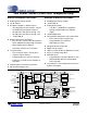
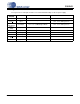
1.1 Digital I/O Pin Characteristics
The logic level for each input should not exceed the maximum ratings for the VL power supply.
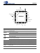
Pin Name
SW/(HW)
I/O Driver Receiver
RESET Input
- 1.8 V - 3.3 V
SCL/CCLK
(I²S/LJ
)
Input
- 1.8 V - 3.3 V, with Hysteresis
SDA/CDIN
(MCLKDIV2)
Input/Output
1.8 V - 3.3 V, CMOS/Open Drain 1.8 V - 3.3 V, with Hysteresis
AD0/CS
(DEM)
Input
- 1.8 V - 3.3 V
MCLK Input
- 1.8 V - 3.3 V
LRCK Input/Output
1.8 V - 3.3 V, CMOS 1.8 V - 3.3 V
SCLK Input/Output
1.8 V - 3.3 V, CMOS 1.8 V - 3.3 V
SDOUT
(M/S
)
Input/Output
1.8 V - 3.3 V, CMOS 1.8 V - 3.3 V
SDIN Input
- 1.8 V - 3.3 V
Table 1. I/O Power Rails